Method of mfg. electronic device with wiring connection structure
A technology for connecting structures and electronic devices, used in semiconductor/solid-state device manufacturing, electrical components, circuits, etc., and can solve problems such as poor contact
- Summary
- Abstract
- Description
- Claims
- Application Information
AI Technical Summary
Problems solved by technology
Method used
Image
Examples
Embodiment 1
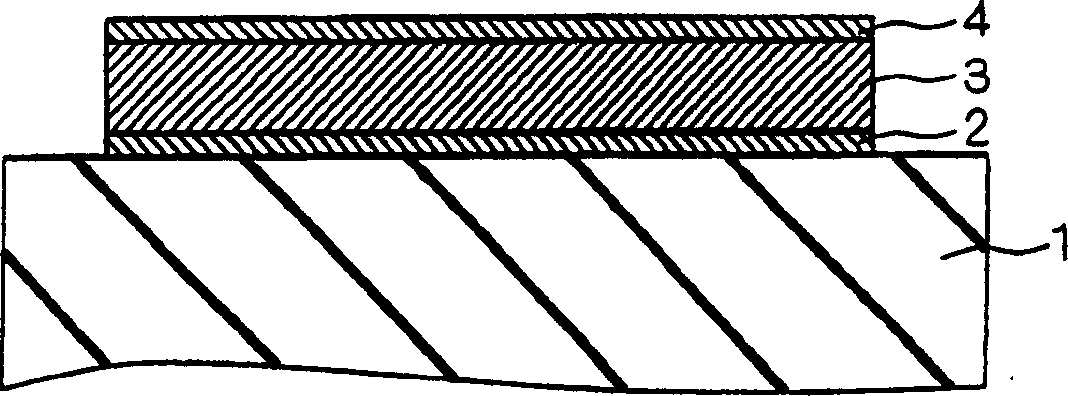
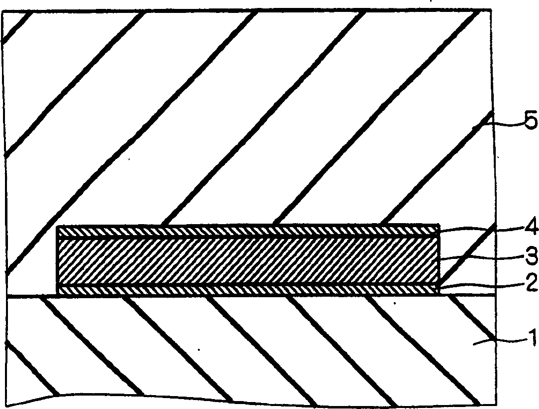
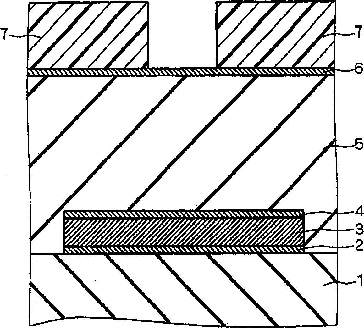
[0046] Figure 1 to Figure 9 It is a diagram showing the manufacturing method of the electronic device having the wiring connection structure according to the first embodiment of the present invention step by step. Figure 1-7 , 9 is a sectional view, Figure 8 is about along Figure 7 Top view at line VIII-VIII shown.
[0047] refer to figure 1 First, a titanium (Ti) film, a titanium nitride (TiN) film, or an undercoat film composed of laminated films thereof is formed entirely on the surface of the interlayer insulating film 1 by PVD. Then, a metal film made of an aluminum alloy such as Al—Cu, Al—Si—Cu, or Al—Cu—Ti is formed entirely on the surface of the lower cladding film by PVD. Next, an overcoat film made of titanium nitride is formed entirely on the surface of the metal film by PVD. The overcoat film functions as an anti-reflection film. Thereafter, these films are patterned by photolithography and anisotropic dry etching to form a first metal wiring composed of ...
Embodiment 2
[0059] Titanium contained in the barrier metal film 9 is soluble in hydrofluoric acid. Therefore, in the cleaning process with hydrofluoric acid, if the barrier metal film 9 is completely dissolved, even if no gap is generated between the barrier metal film 9 and the side wall of the via hole 8, the cleaning liquid will pass through the dissolved barrier layer. The gap created behind the metal film 9 penetrates into the metal film 3 .
[0060] In order to avoid this problem, in the present embodiment 2, the depth D of the through hole 8 (referring to Figure 4 ) is set at a depth at which the barrier metal film 9 formed on the side wall of the via hole 8 cannot be completely dissolved by cleaning.
[0061] Specifically, Figure 7 The cleaning after the CMP step shown is cleaning with dilute hydrofluoric acid for about 5 to 30 seconds. This also depends on the film-forming method of the barrier metal film 9, but during this period of time, the dissolution of the barrier meta...
Embodiment 3
[0064] Figure 10 11 is a cross-sectional view showing the manufacturing method of the electronic device with the wiring connection structure according to the third embodiment of the present invention step by step. In the figure, in particular, the vicinity of the bottom surface of the through hole 8 related to the etching process for forming the through hole 8 is shown enlarged.
[0065] In the above-mentioned embodiment 1, such as Figure 4 As shown, the via hole 8 is realized by penetrating the upper coating film and reaching the metal film 3 . In contrast to this, in this embodiment 3, as Figure 10 As shown, the anisotropic dry etching for forming the via hole 8 is stopped when the surface of the upper cladding film 4 is exposed. As a result, the bottom surface of the via hole 8 is defined by the surface of the upper cladding film 4, and the metal film 3 is not exposed.
[0066] refer to Figure 11 , and then, via plugs were formed through the same steps as in the fi...
PUM
 Abstract
Description
Claims
Application Information


