
Semiconductor device and producing method thereof

A manufacturing method and semiconductor technology, applied in the field of diffusion layer, can solve the problems of low-impedance extended diffusion layer, enlargement, difficulty in forming shallow joints, etc., and achieve the effects of shallow extended diffusion layer, shallow resistance, and reduction of redundant point defects

Active Publication Date: 2004-09-08
GK BRIDGE 1
View PDF1 Cites 9 Cited by
  • Summary
  • Abstract
  • Description
  • Claims
  • Application Information

AI Technical Summary

Problems solved by technology

[0014] Therefore, even if the implantation energy of the ion implantation is lowered in order to obtain a shallower junction in the above-mentioned conventional manufacturing method of a semiconductor device, the TED of the implanted dopant will become larger. In the case of low-energy implantation, it is difficult to form MIS-type transistors with shallow junctions and low-resistance extended diffusion layers

Method used


Image

  • Semiconductor device and producing method thereof
  • Semiconductor device and producing method thereof
  • Semiconductor device and producing method thereof

Examples


no. 1 Embodiment

[0046] A first embodiment of the present invention will be described below with reference to the drawings.

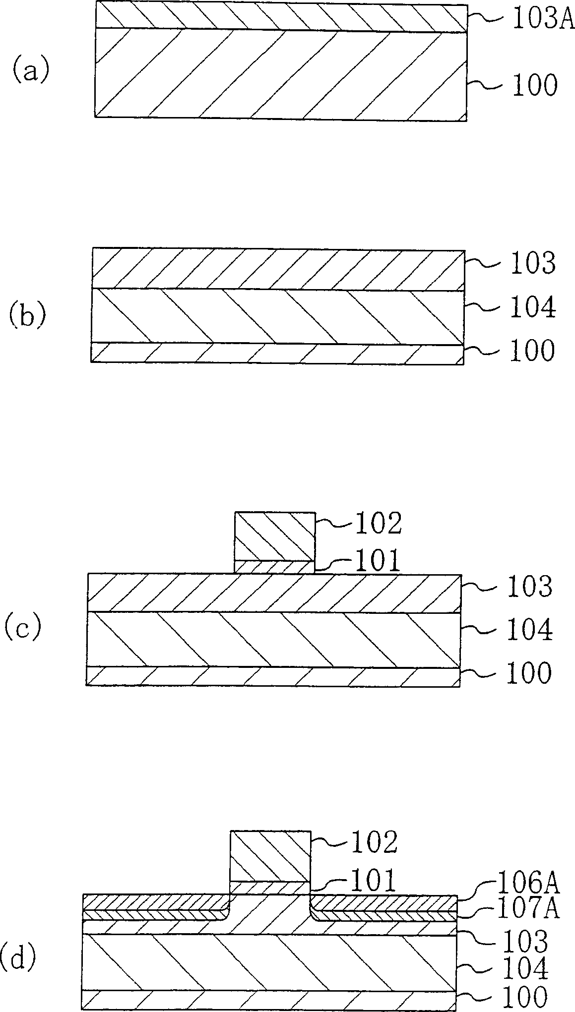
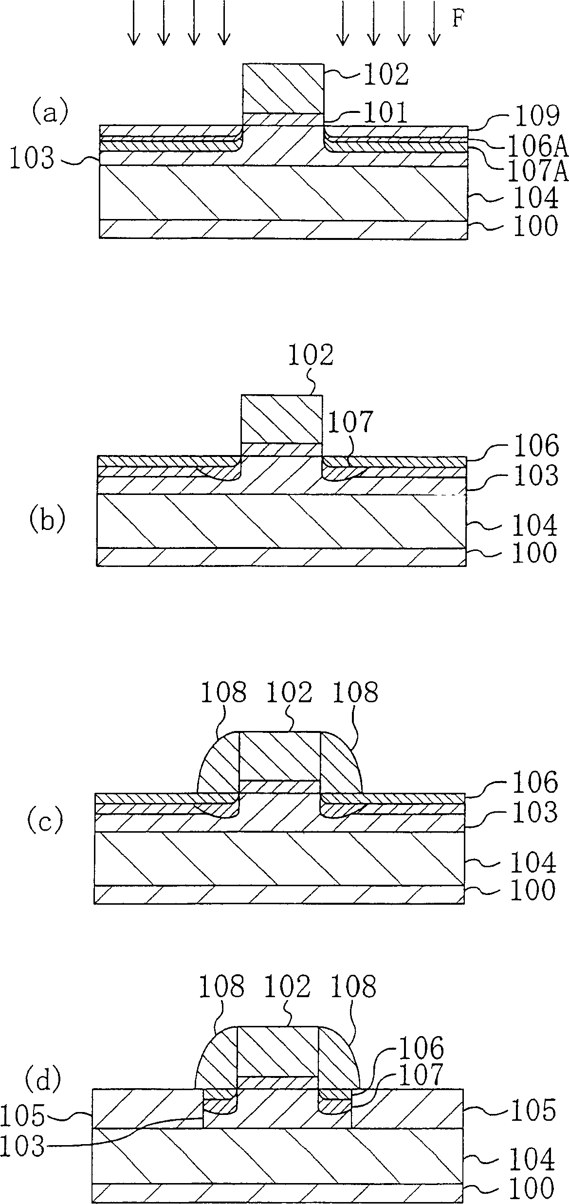
[0047] figure 1 (a)~ figure 1 (d) and figure 2 (a)~ figure 2 (d) A cross-sectional structure showing the sequence of steps in the method for manufacturing a semiconductor device according to the first embodiment of the present invention.

[0048] First, if figure 1 As shown in (a), in the channel formation region of the semiconductor substrate 100 made of P-type silicon, the implantation energy is 140keV and the implantation dose is 5×10 12 / cm 2 Under the implantation conditions of , arsenic (As) ions, which are N-type impurities, are ion-implanted to form an N-type channel implantation layer 103A on the upper portion of the semiconductor substrate 100 . Thereafter, in the N-type well formation region of the semiconductor substrate 100, at an implantation energy of 260 keV and an implantation dose of 1×10 13 / cm 2 Under the first implantation conditions, p...

no. 2 Embodiment

[0070] Hereinafter, a second embodiment of the present invention will be described with reference to the drawings.

[0071] Figure 4 (a)~ Figure 4 (e) and Figure 5 (a)~ Figure 5 (d) A cross-sectional structure showing the sequence of steps of the method for manufacturing a semiconductor device according to the second embodiment of the present invention.

[0072] First, if Figure 4 As shown in (a), by implanting energy at 70keV and implanting dose at 5×10 12 / cm 2 Under certain implantation conditions, arsenic (As) ions, which are N-type impurities, are ion-implanted into the channel formation region of the semiconductor substrate 100 made of P-type silicon, thereby forming an N-type channel implantation in the upper part of the semiconductor substrate 100. Layer 103A. Afterwards, by implanting energy at 260keV and implanting dose at 1×10 13 / cm 2 Under the first implantation conditions of the semiconductor substrate 100, phosphorus (P) ions, which are N-type impu...

no. 3 Embodiment

[0092] A third embodiment of the present invention will be described below with reference to the drawings.

[0093] Figure 7 (a)~ Figure 7 (e) and Figure 8 (a)~ Figure 8 (d) A cross-sectional structure showing the sequence of steps of the method for manufacturing a semiconductor device according to the third embodiment of the present invention.

[0094] First, if Figure 7 As shown in (a), by implanting energy at 70keV and implanting dose at 5×10 12 / cm 2 Under implantation conditions, arsenic (As) ions are ion-implanted as an N-type impurity into the channel formation region of the semiconductor substrate 100 made of P-type silicon, thereby forming an N-channel implantation layer 103A on the upper portion of the semiconductor substrate 100. . Afterwards, by implanting energy at 260keV and implanting dose at 1×10 13 / cm 2 Under the first implantation conditions of the semiconductor substrate 100, phosphorus (P) ions, which are N-type impurities, are ion-implanted ...


PUM


Abstract

An n-type channel diffused layer and an n-type well diffused layer are formed in the top portion of a semiconductor substrate, and a gate insulating film and a gate electrode are formed on the semiconductor substrate. Using the gate electrode as a mask, boron and arsenic are implanted to form p-type extension implanted layers and n-type pocket impurity implanted layers. Fluorine is then implanted using the gate electrode as a mask to form fluorine implanted layers. The resultant semiconductor substrate is subjected to rapid thermal annealing, forming p-type high-density extension diffused layers and n-type pocket diffused layers. Sidewalls and p-type high-density source / drain diffused layers are then formed.

Description

technical field [0001] The present invention relates to a semiconductor device and a method for manufacturing the same, and more particularly, to a semiconductor device and a method for manufacturing the semiconductor device that can be miniaturized and has a diffusion layer with a shallow junction surface and low resistance. Background technique [0002] With the high integration of semiconductor integrated circuits, miniaturization of MIS transistors is increasingly required. In order to achieve this goal, MIS transistors having extended diffusion layers with shallow junctions and low impedance have been sought. [0003] Hereinafter, a conventional method of manufacturing a semiconductor device will be described with reference to the drawings (for example, see Patent Document 1). [0004] Figure 9 (a)~ Figure 9 (e) shows the cross-sectional structure of the manufacturing process of the conventional semiconductor device manufacturing method. [0005] First, in Figure 9 ...

Claims


Application Information

Patent Timeline
Patent Type & Authority Applications(China)
IPC IPC(8): H01L21/265H01L21/28H01L21/324H01L21/336H01L29/06H01L29/49H01L29/51H01L29/78
CPCH01L29/7833H01L29/51H01L21/28194H01L29/518H01L29/6659H01L29/495H01L21/324H01L21/26506H01L29/517H01L21/28202H01L21/2658H01L21/26513
Inventor 野田泰史
Owner GK BRIDGE 1
Learn More