Contact hole shaping method, thin-membrane semiconductor producing method, electronic device and producing method thereof

A thin-film semiconductor and contact hole technology, used in semiconductor/solid-state device manufacturing, semiconductor devices, electrical components, etc., can solve the problems of high price, difficult to remove photoresist, long time, effort and energy, etc., to reduce costs , the effect of saving time and energy

Inactive Publication Date: 2004-09-22
SEIKO EPSON CORP
View PDF1 Cites 7 Cited by
  • Summary
  • Abstract
  • Description
  • Claims
  • Application Information

AI Technical Summary

Problems solved by technology

Therefore, the conventional method of forming a contact hole requires an expensive vacuum device in order to dry etch the insulating film.
Moreover, since the process using a vacuum device requires a lot of time, effort and energy to form the contact hole, the maintenance of the vacuum device is not easy.
[0006] In addition, during dry etching, plasma damage (plasma damage) caused by the impact of charged particles on the substrate or charge accumulation on the substrate surface occurs, and there is a problem that the electrical characteristics of the semiconductor device are deteriorated.
Furthermore, during dry etching, there is a problem that it is difficult to sufficiently ensure the selectivity ratio of the insulating film and the conductive film of the lower layer, and the conductive film of the lower layer is etched, and the problem of resistive electrical conduction cannot be achieved.
In addition, there is a problem that the photoresist is hardened during dry etching, and it is difficult to remove the photoresist after etching.

Method used


Image

  • Contact hole shaping method, thin-membrane semiconductor producing method, electronic device and producing method thereof
  • Contact hole shaping method, thin-membrane semiconductor producing method, electronic device and producing method thereof
  • Contact hole shaping method, thin-membrane semiconductor producing method, electronic device and producing method thereof

Examples


Embodiment Construction

[0034] Hereinafter, embodiments of the present invention will be described with reference to the drawings.

[0035] The method for forming a contact hole of the present invention and the best embodiment of an electronic device manufactured by the method will be described in detail with reference to the accompanying drawings.

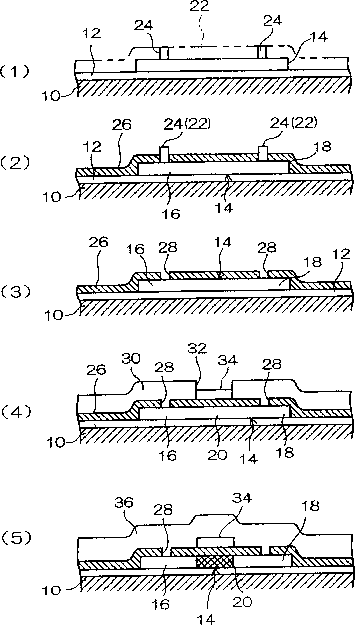
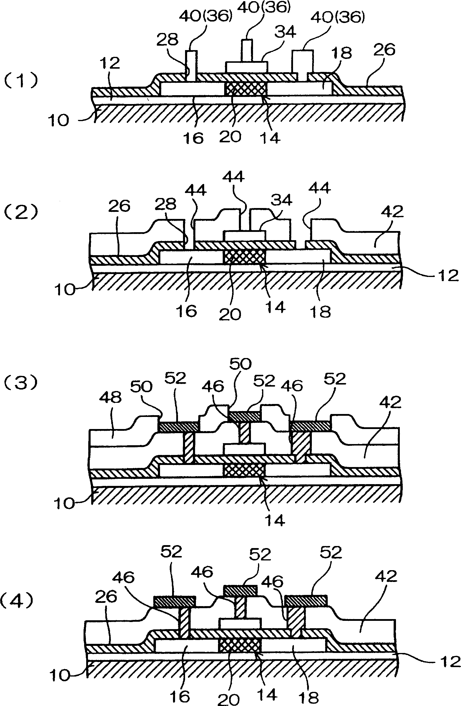
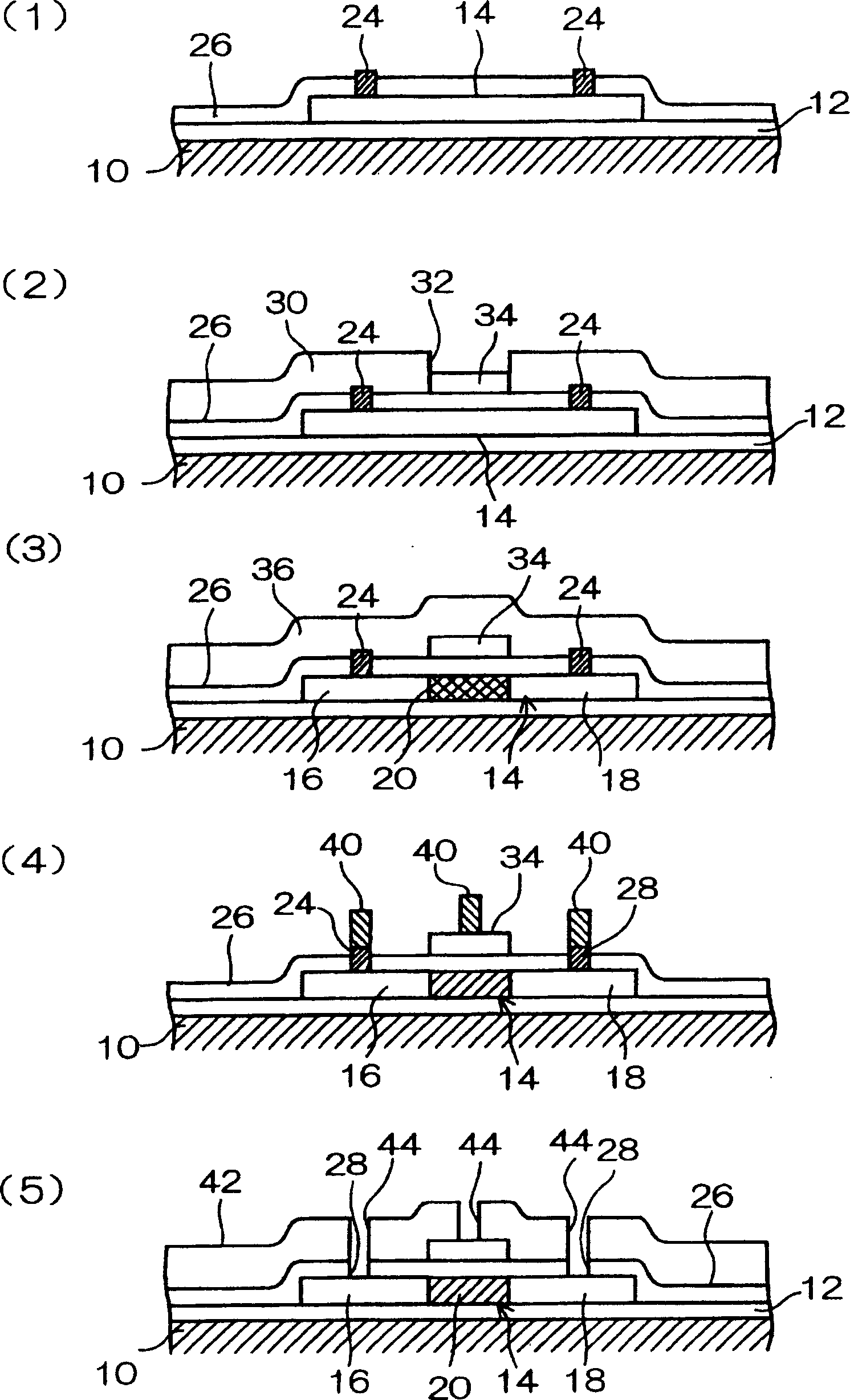
[0036] figure 1 , figure 2 It is an example of the manufacturing process of the electronic device using the contact hole forming method of 1st Embodiment of this invention. This manufacturing process is a process using the contact hole forming method of the embodiment when forming a switching circuit such as a liquid crystal panel, and is a process diagram of a method of connecting a thin film transistor (TFT) made of low temperature polysilicon (LTPS) and wiring.

[0037] First, if figure 1 As shown in (1), an underlying insulating film 12 of silicon dioxide or the like is formed on the surface of the glass substrate 10 . The underlying insulating ...


PUM


Abstract

Provided is a method by which contact holes can be formed without using a vacuum device. In this method, mask pillars 40 are formed by exposing and developing resist films at positions corresponding to contact hole forming areas on a source region 16 and a drain region 18 of a polycrystalline silicon film 14 and a gate electrode 34. Then an insulating layer 42 is formed by applying a liquid insulating material to the whole surface of a glass substrate 10 excluding the mask pillars 40. Thereafter, second contact holes 44 and first contact holes 28 are formed through the insulating layer 42 and a gate insulating film 26 by ashing the mask pillars 40.

Description

technical field [0001] The present invention relates to a method of forming a contact hole formed on an interlayer insulating film or the like of a semiconductor device, a method of manufacturing a thin-film semiconductor device, a method of manufacturing an electronic device, and an electronic device. Background technique [0002] In recent years, semiconductor devices as electronic devices have been multilayered in order to achieve high integration. Furthermore, in a semiconductor device having multilayer wiring, when upper and lower wiring patterns arranged through an interlayer insulating film are electrically connected, a contact hole is formed in the interlayer insulating film and is performed through the contact hole. Conventionally, contact holes are generally formed as described in Patent Document 1 as follows. [0003] First, a conductive material such as metal is deposited on a substrate and etched to form a lower wiring layer. Next, an interlayer insulating fil...

Claims


Application Information

Patent Timeline
Patent Type & Authority Applications(China)
IPC IPC(8): H01L21/28H01L21/336H01L21/768H01L29/417H01L29/423H01L29/45H01L29/49H01L29/786
CPCH01L29/66757H01L21/76802H01L29/4908H01L29/458H01L29/42384H01L29/41733H01L21/28
Inventor 佐藤充汤田坂一夫
Owner SEIKO EPSON CORP
Why Eureka
Try Eureka