

Electric field luminous display device and its mfg. method
An electroluminescence and display device technology, applied in electroluminescence light sources, electric light sources, lighting devices, etc., can solve problems such as peeling, floating, cracking of desiccant layers, and damage to organic EL components.
- Summary
- Abstract
- Description
- Claims
- Application Information
AI Technical Summary
Problems solved by technology
Method used
Image

Examples
no. 1 Embodiment approach
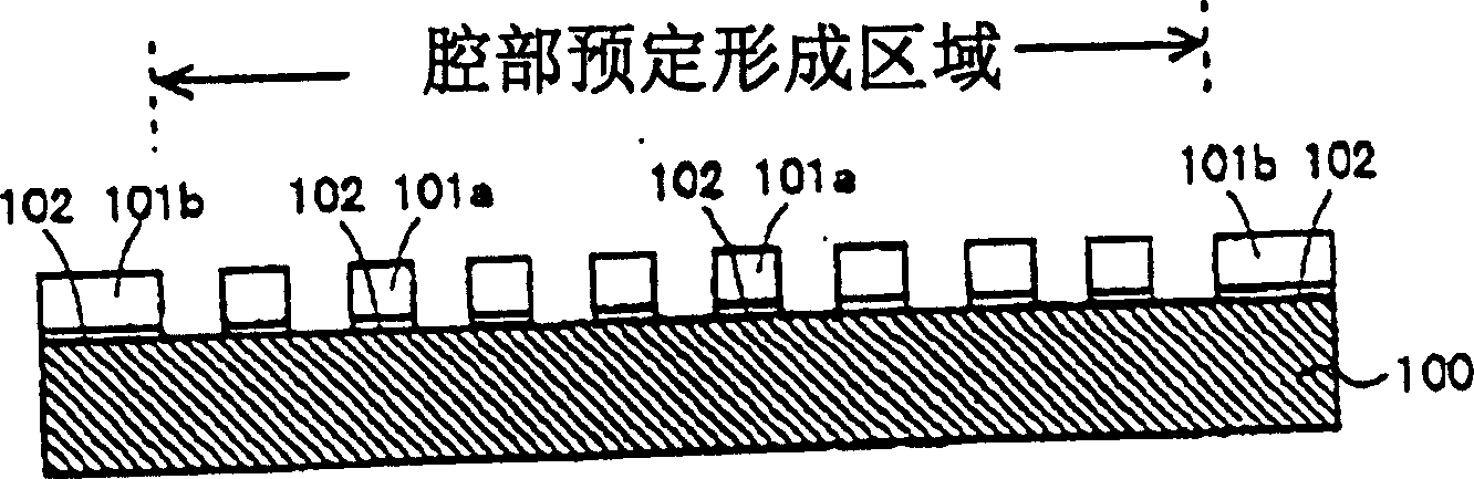
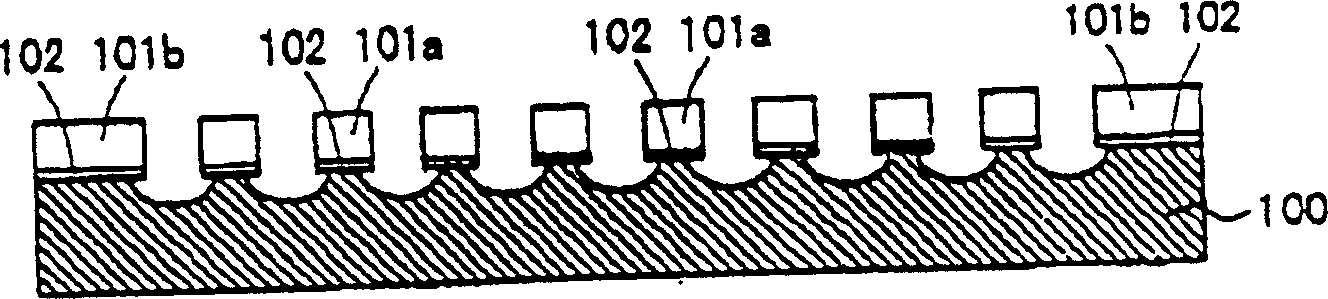
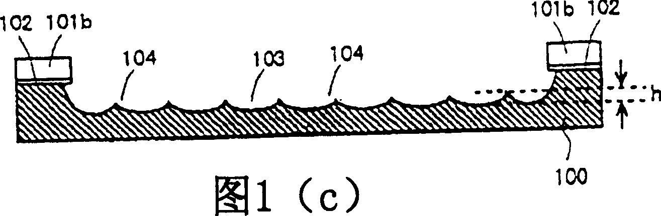
[0046]FIG. 1 is a cross-sectional view sequentially showing manufacturing steps (a) to (e) of the electroluminescence display device according to the first embodiment of the present invention. 2 is a plan view of an electroluminescence display device, the X-X line sectional view of FIG. 2(a) is FIG. 1(a), and the Y-Y line sectional view of FIG. 2(b) is FIG. 1(e).
[0047] Hereinafter, a method of manufacturing the electroluminescent display device according to the first embodiment will be described. First, as shown in FIG. 1( a ) and FIG. 2( a ), a sealing glass substrate 100 having a thickness of about 0.7 mm is prepared. A plurality of resist film patterns 101 a arranged in a grid pattern are formed in a region to be formed of a cavity portion of the sealing glass substrate 100 (hereinafter referred to as a region to be formed in a cavity portion). Then, a ring-shaped resist film pattern 101b is formed around the region where the cavity portion is to be formed. A chrome ma...
no. 2 approach
[0053] FIG. 3 is a cross-sectional view sequentially showing the manufacturing process of the electroluminescent display device according to the second embodiment of the present invention. In addition, in the figure, the same code|symbol is attached|subjected to the same component as FIG. 1.
[0054] First, as shown in FIG. 3( a ), a sealing glass substrate 100 having a thickness of approximately 0.7 mm is prepared. And a resist film pattern 101c having an opening is formed in a region to be formed of a cavity of the sealing glass substrate 100 (hereinafter referred to as a region to be formed of a cavity). The resist film pattern 101c is a ring-shaped resist film pattern formed on the periphery of the region where the cavity portion is to be formed. As in the first embodiment, it is preferable to form the chrome mask layer 102 on the bottom layer of the resist film pattern 101c. In addition, a hydrofluoric acid-resistant film can also be used for patterning.
[0055] Next,...
no. 3 approach
[0060] 4 is a cross-sectional view sequentially showing the manufacturing process of the electroluminescence display device according to the third embodiment of the present invention. In addition, in the figure, the same components as those in FIG. 1 are denoted by the same symbols.
[0061] First, as shown in FIG. 4( a ), a sealing glass substrate 100 having a thickness of about 0.7 mm is prepared. And a resist film pattern 101d having an opening is formed in a region to be formed of the cavity of the sealing glass substrate 100 (hereinafter referred to as a region to be formed of the cavity). The resist film pattern 101d is a ring-shaped resist film pattern formed on the periphery of the region where the cavity portion is to be formed. A chromium mask layer 102 may be formed under the resist film pattern 101d. In addition, a hydrofluoric acid-resistant film can also be used for patterning.
[0062] As shown in FIG. 4( b ), the cavity portion 120 is formed by etching the s...
PUM
| Property | Measurement | Unit |
|---|---|---|
| Thickness | aaaaa | aaaaa |
Abstract
Description
Claims
Application Information