Pad structure and manufacturing method thereof

A pad and metal pad technology, applied in semiconductor/solid-state device manufacturing, electrical components, electrical solid-state devices, etc., can solve problems such as insufficient bonding force, impact on device performance and yield, and pad drop-off

Inactive Publication Date: 2015-09-30
SEMICON MFG INT (SHANGHAI) CORP
View PDF5 Cites 6 Cited by
  • Summary
  • Abstract
  • Description
  • Claims
  • Application Information

AI Technical Summary

Problems solved by technology

[0006] A study was conducted on the problem of pad falling off or upturning, and it was found that the problem was due to the weak bonding force between the top metal layer and the pad, and the bonding force was not strong enough to cause the above problem
[0007] Therefore, in the prior art, the top metal layer and the bonding pa

Method used


Image

  • Pad structure and manufacturing method thereof
  • Pad structure and manufacturing method thereof
  • Pad structure and manufacturing method thereof

Examples


Embodiment 1

[0073] Attached below Figure 3a and 3b The pad structure described in a specific implementation manner of the present invention will be further described.

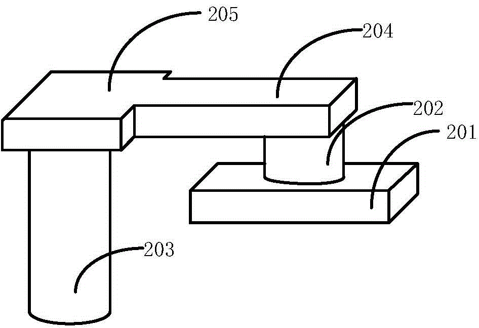
[0074] in Figure 3a It is a schematic diagram of the three-dimensional structure of the bonding pad in a specific embodiment of the present invention; Figure 3b It is a schematic cross-sectional view of the bonding pad in a specific embodiment of the present invention.

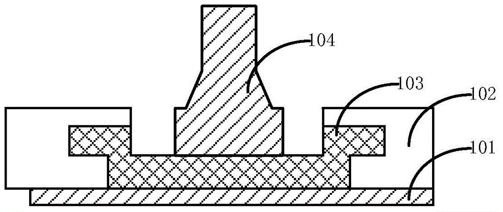
[0075] Specifically, the pad structure includes a metal pad 205, metal lines 202, 204, a top metal layer 201, a nail pad 203, and an isolation material layer.

[0076] Wherein, the metal pad 205 is an Al pad, but it is not limited to one type of Al pad, and those skilled in the art may select other commonly used metal pads.

[0077] The shape of the metal pad 205 can be square, such as Figure 3a As shown, it can be a rectangle or a square. In addition, other shapes, such as rhombus, triangle or polygon, can also be used, and other irregular patter...

Embodiment 2

[0097] The invention also provides a preparation method of the pad structure.

[0098] First, step 201 is performed to provide a base, which at least includes a semiconductor substrate (not shown in the figure), on which various active devices and interconnection structures are formed, and the semiconductor substrate may be At least one of the materials mentioned below: silicon, silicon-on-insulator (SOI), silicon-on-insulator (SSOI), silicon-germanium-on-insulator (S-SiGeOI), and silicon-germanium-on-insulator (SiGeOI), etc. . A doped region and / or an isolation structure may be formed in the substrate, and the isolation structure is a shallow trench isolation (STI) structure or a local oxide of silicon (LOCOS) isolation structure.

[0099] Step 202 is executed to form an interlayer dielectric layer 206 on the substrate.

[0100] Specifically, an interlayer dielectric layer 206 is deposited on the substrate, and the interlayer dielectric layer 206 may be a metal interlayer d...


PUM


Abstract

The invention relates to a pad structure and a manufacturing method thereof. The pad structure comprises an isolation material layer, a metallic pad situated above the isolation material layer, a top metallic layer embedded in the isolation material layer and connected with the metallic pad through a metallic connecting line, and a nail pad situated under the metallic pad, tightly connected with the metallic pad and embedded in the isolation material layer while being spaced apart from the top metallic layer. The invention solves the problems in the prior art and provides a new pad structure. The nail pad is situated under the metallic pad, and the nail pad is integrated into one body with the metallic pad and embedded tightly in a passivation layer under the metallic pad. The bonding force of the metallic pad is thus increased to prevent falling off of the metallic pad.

Description

technical field [0001] The present invention relates to the field of semiconductors, in particular, the present invention relates to a bonding pad structure and a preparation method thereof. Background technique [0002] With the continuous improvement of semiconductor manufacturing technology and the continuous reduction of the size of semiconductor devices, the size of integrated circuit devices is continuously reduced. In the back-end process (The back end of line, BEOL), welding wire bonding technology is a widely used method for connecting semiconductor dies with circuits to pins on the original package to realize I / O (in / out) connection, wherein the size of the wire bond pads and the arrangement and layout of the leads determine the final size of the integrated circuit device. [0003] Metal wire materials and metal wire bonding processes are widely used in the packaging of high-end integrated circuits in the field of integrated circuit packaging due to their good me...

Claims


Application Information

Patent Timeline
IPC IPC(8): H01L23/498H01L21/48
CPCH01L24/05H01L2224/04042H01L2224/48463
Inventor 张贺丰
Owner SEMICON MFG INT (SHANGHAI) CORP
Why Eureka
Try Eureka