Multi-chip stacking method for halving routing procedure and structure thereof

A multi-chip and chip technology, which is applied in semiconductor/solid-state device manufacturing, semiconductor devices, semiconductor/solid-state device components, etc., can solve problems such as easy punching of bonding wires and inability to omit wire bonding processes, etc., to achieve narrow gaps, The effect of reducing chip stack height and enhancing bonding force

Inactive Publication Date: 2009-10-07
POWERTECH TECHNOLOGY
View PDF0 Cites 7 Cited by
  • Summary
  • Abstract
  • Description
  • Claims
  • Application Information

AI Technical Summary

Problems solved by technology

[0004] Since the first chip 120 and the second chip 140 are respectively connected to the carrier 110 by dedicated first bonding wires 131 and second bonding wires 132, In the process, it needs to go through two wire bonding, corresponding to the number of chip stacks, to achieve the electrical interconnection between the first chip 120, the second chip 140 and the carrier 110, so the multi-channel wire bonding process cannot be omitted
Moreover, too many welding wires in the crowded sealing space are prone to the problem of punching wires
In addition, it is known that these bonding wires 131 and 132 are all bonded in the forward direction, so as to avoid the phenomenon of false soldering or empty soldering on the joints on the chip, but the maximum arc height of these bonding wires 131 is above the first chip 120. superior

Method used


Image

  • Multi-chip stacking method for halving routing procedure and structure thereof
  • Multi-chip stacking method for halving routing procedure and structure thereof
  • Multi-chip stacking method for halving routing procedure and structure thereof

Examples


no. 1 Embodiment

[0090] According to the first specific embodiment of the present invention, with reference to Figure 4 and Figure 5 , specifically disclosing a multi-chip stacking method in which the wire bonding process is halved.

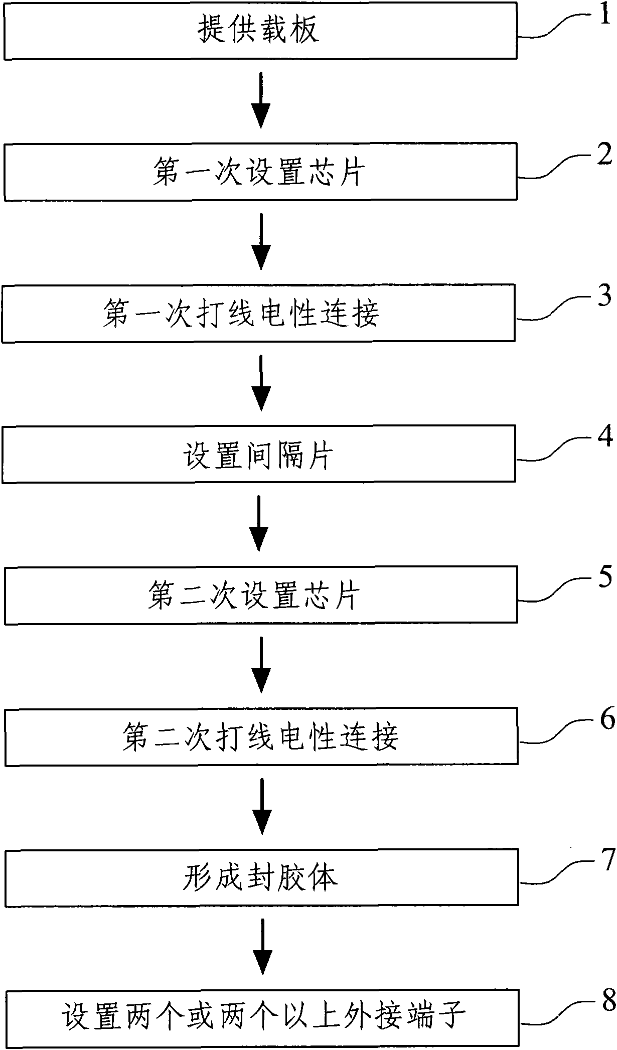
[0091] see Figure 4 As shown, a multi-chip stacking method mainly includes the following steps: Step 11, providing a carrier board; Step 12, setting up chips for the first time; Step 13, making electrical connections with wires; Step 14, forming a filling glue; Step 15, the first Secondary setting of chips and electrical connection; Step 16, forming a sealing body; Step 17, setting two or more external terminals. Among them, the step 14 of "forming the filling glue" is an unnecessary step, so in different embodiments, the step 14 of "forming the filling glue", the step 16 of "forming the sealing body" and the step of "setting two or more circumscribed Terminal" step 17 can be omitted or replaced. The component composition relationship in each step can be f...

no. 2 Embodiment

[0106] According to the second embodiment of the present invention, another multi-chip stacking method and structure that reduces the wiring process by half is disclosed.

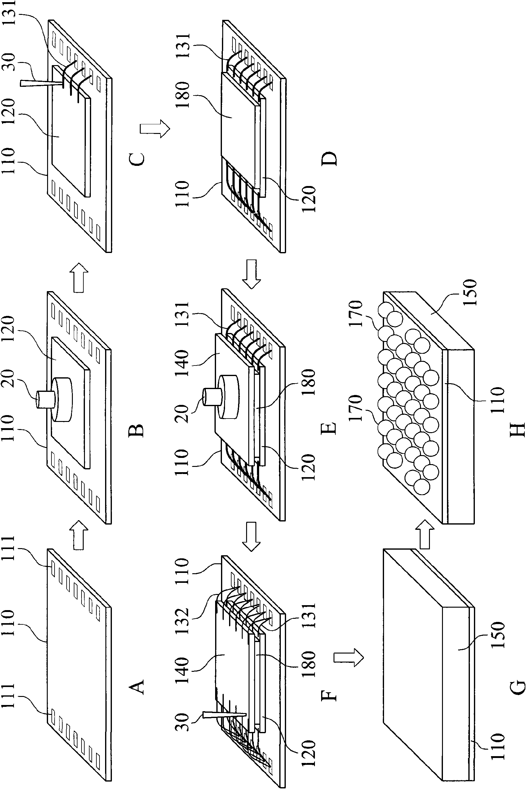
[0107] First, see Figure 10 As shown in Figure A, a carrier board 310 is provided, and the carrier board 310 has two or more fingers 311 . In this embodiment, the fingers 311 can be formed in the central area of ​​the carrier 310 .

[0108] Afterwards, see Figure 10 Figure B in and Figure 11 As shown, at least one first chip 320 is set on the carrier 310 by using the chip suction nozzle 40. In this embodiment, the first chip 320 can be two or more, and the fingers 311 are located on these first chips. Between the chips 320 , these fingers 311 can be shared by wire bonding, so the number of these fingers 311 can be reduced to reduce the cost of the carrier 310 . Such as Figure 11 As shown, each first chip 320 has two or more than two first electrodes 321 . The first electrodes 321 can be arranged i...


PUM


Abstract

The invention discloses a multi-chip stacking method for halving routing procedure, comprising the following steps: firstly, providing a support plate having two or more finger joints and arranging at least one first chip on the support plate; then, routing to form two or more bonding wires to connect a first electrode of the first chip to the finger joints; arranging at least one second chip on the first chip face to face, and meanwhile, joining the second electrode of the second chip to one end of the bonding wires on the first electrodes, so that the second chip is electrically connected to the support plate through the bonding wires. The invention also discloses a multi-chip stacking structure for halving routing procedure. Therefore, the invention can shorten the procedure period and save cost, ensures that the bonding wires are located at the routing end on the chip and connected to the first electrode, and avoids line disconnection and line breasting.

Description

technical field [0001] The present invention relates to a multi-chip stacking technology applicable to semiconductor devices, in particular to a multi-chip stacking method and structure which halves the wiring process. Background technique [0002] In order to improve the performance and capacity of a single semiconductor device to meet the trend of miniaturization, large capacity and high speed of electronic products, generally speaking, multiple chips are stacked on the carrier board to save space. However, the number of wire bonding electrical connections in the process corresponds to the number of chip stacks. When the number of chip stacks increases, the number of wire bonding electrical connections also increases, making the process complicated and prone to wire punching problems. [0003] see figure 1 shown and with reference to figure 2 , a known multi-chip stacking method includes the following steps: Step 1, providing a carrier board; Step 2, setting the chips f...

Claims


Application Information

Patent Timeline
Patent Type & Authority Applications(China)
IPC IPC(8): H01L21/60H01L25/00H01L23/488
CPCH01L2924/01013H01L2224/451H01L2924/01005H01L2924/01082H01L2924/01033H01L2224/32225H01L2924/01079H01L2224/48465H01L2224/48091H01L2924/15311H01L2224/48227H01L2924/014H01L2224/73265H01L2224/48471H01L2224/16145H01L2924/0105H01L24/48H01L2924/01029H01L2224/73204H01L2224/16H01L2924/01006H01L2224/32145H01L2224/85207H01L24/73H01L2924/181H01L2224/48H01L2924/00014H01L2924/00H01L2924/00012
Inventor 钟启源
Owner POWERTECH TECHNOLOGY
Why Eureka
Try Eureka