Boundary scan testing device for integrated circuit

A technology of boundary scan testing and integrated circuits, applied in the direction of measuring devices, measuring electricity, measuring electrical variables, etc., can solve problems such as expensive, difficult to promote, complex structure, etc., achieve low cost, easy to promote, and improve the pass rate.

Inactive Publication Date: 2004-11-03
徐州铁手五金工具制造有限公司
View PDF2 Cites 25 Cited by
  • Summary
  • Abstract
  • Description
  • Claims
  • Application Information

AI Technical Summary

Problems solved by technology

The content of the invention is a dedicated boundary-scan test device, which can perform combinational logic tests on boundary-scan devices, focusing on the functional test of the circuit itse

Method used


Image

  • Boundary scan testing device for integrated circuit
  • Boundary scan testing device for integrated circuit
  • Boundary scan testing device for integrated circuit

Examples


Embodiment Construction

[0018] The specific implementation manner of the present invention will be described below in conjunction with the accompanying drawings.

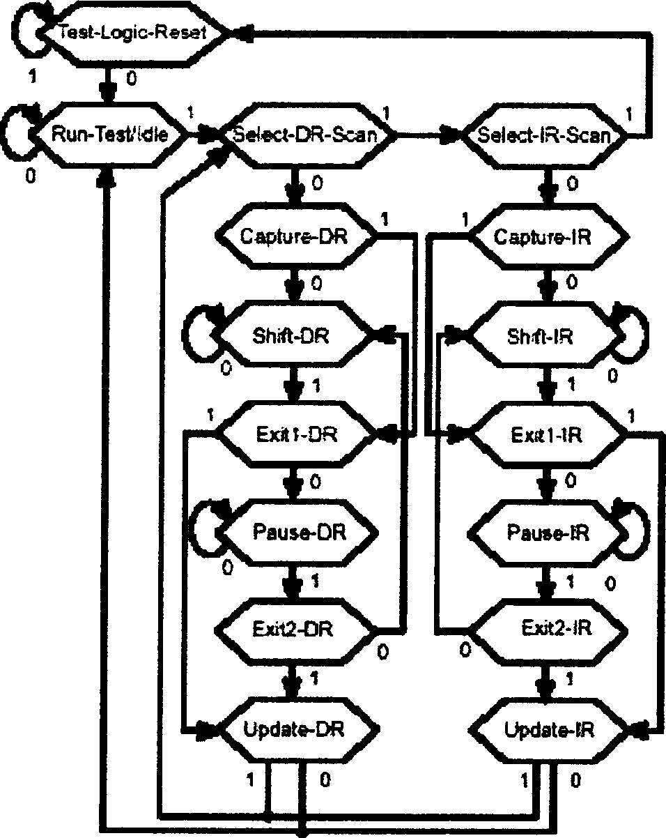
[0019] figure 1 It is the state flow diagram of the TAP controller defined by IEEE 1149.1. It is the principle basis of the present invention.

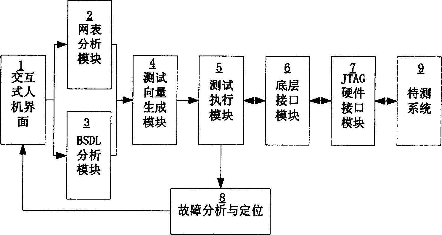
[0020] figure 2 It is an embodiment and a working flow chart of the device of the present invention. When the human-computer interaction interface 1 is started, the program of the initialization part of the program is started at the same time. Input the PCB netlist file and BSDL file, and perform the analysis of the two types of files respectively: netlist file analysis module 2 and BSDL file analysis module 3. Then execute the test vector generating module 4 to generate test vectors according to the analysis results of the two types of files. The test execution module 5 sends the test vector to the system under test 9 through the bottom layer interface module 6 and the JTAG hardware interfa...


PUM


Abstract

The integrated circuit boundary scanning measurement device is used in measuring integrated circuit on printed circuit board in communication electronic technology. The boundary scanning measurement device utilizing the parallel port of computer includes bottom interface module, initializing module, measurement vector producing module, measurement module, fault analyzing and locating module, and boundary scanning describing language file analysis module. Boundary scanning measurement is completed via making full use of the PC resource, i. e., compiling PC boundary scanning application program, utilizing the parallel port in PC and assisting with the JTAG interface hardware unit. The present invention can complete the boundary scanning measurement of devices in printed circuit board and the whole printed circuit board. The present invention can raise the measurement capacity of printed circuit boards.

Description

Technical field: [0001] The invention belongs to the field of integrated circuit testing on printed circuit boards in the field of communication electronics, and relates to integrated circuits with boundary scan units, large-scale integrated circuits or ultra-large-scale integrated circuits, and integrated circuits with boundary scan functions on printed circuit boards. Testing of interconnections between circuits. Background technique: [0002] The functions of integrated chips (IC: Integrated Circuit) are becoming more and more powerful. With the continuous improvement of technology, it has developed to sub-micron technology. At the same time, there are more and more IC pins. Board) The wiring pitch is getting smaller and smaller, and the structure is getting more and more complex. In this way, the bed-of-nail tested by the mechanical probe is difficult to contact the nodes on the circuit board, and the contact point space left for the bed-of-nail is getting smaller and s...

Claims


Application Information

Patent Timeline
IPC IPC(8): G01R31/30
Inventor 程智刚
Owner 徐州铁手五金工具制造有限公司
Why Eureka
Try Eureka