
Optimized design method of microwave amplifying circuit

A technology for microwave amplification and optimization design, which is applied to high-frequency amplifiers, amplifier input/output impedance improvement, electrical components, etc., can solve the problems of limited automatic optimization function, small number of independent variables, and inability to guarantee global optimality, etc.

Inactive Publication Date: 2005-01-12
TSINGHUA UNIV
View PDF0 Cites 10 Cited by
  • Summary
  • Abstract
  • Description
  • Claims
  • Application Information

AI Technical Summary

Problems solved by technology

However, this design has the following difficulties: 1. The automatic optimization function is limited, and it is easy to fall into a local extreme point and stop automatically; 2. It cannot guarantee the global optimum; 3. To play the EDA software optimization function requires the designer to have rich experience in amplifier design, and to Different active devices require different design experiences; 4. The calculation results are highly dependent on the number of circuit variables, and the number of independent variables is small

Method used


Image

  • Optimized design method of microwave amplifying circuit
  • Optimized design method of microwave amplifying circuit
  • Optimized design method of microwave amplifying circuit

Examples


Embodiment Construction

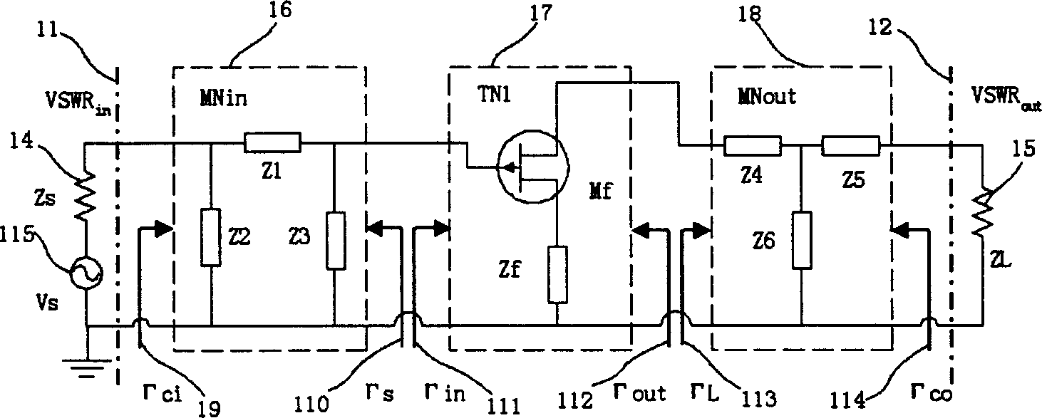
[0094] The CDMA mobile communication amplifier circuit specific design method of one of circuit principle of the present invention and embodiment is described in detail as follows in conjunction with each accompanying drawing:

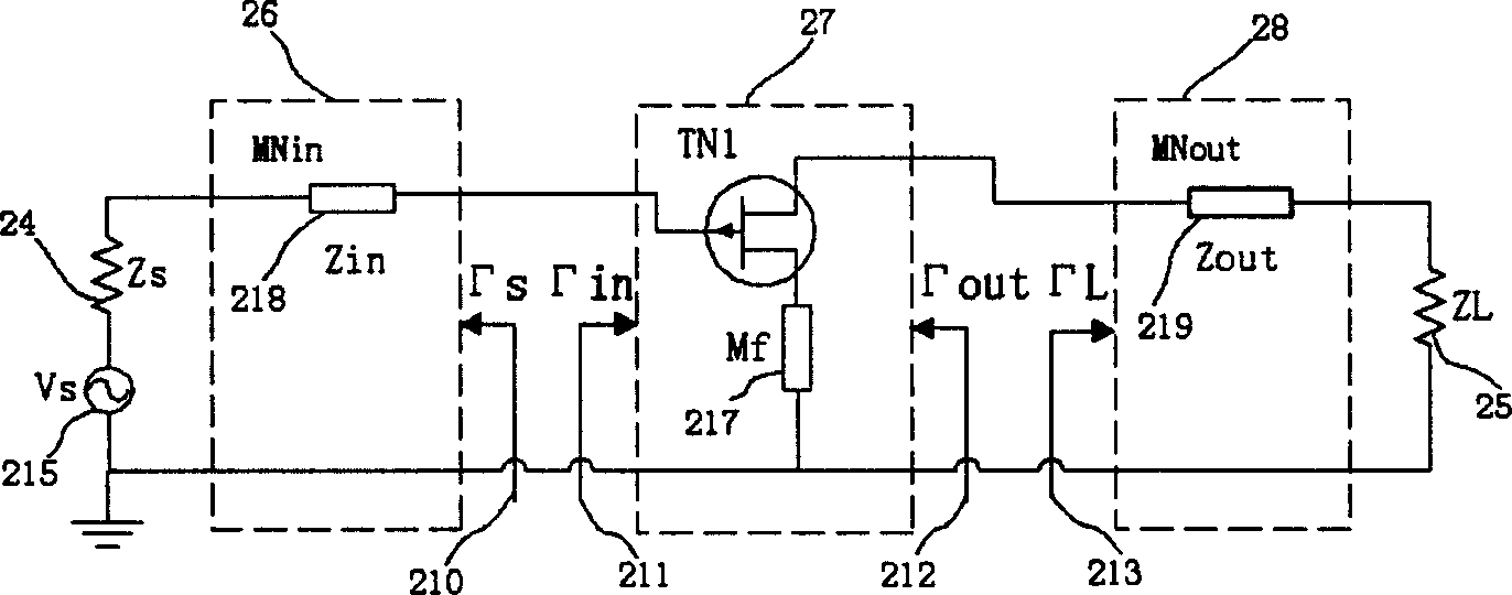
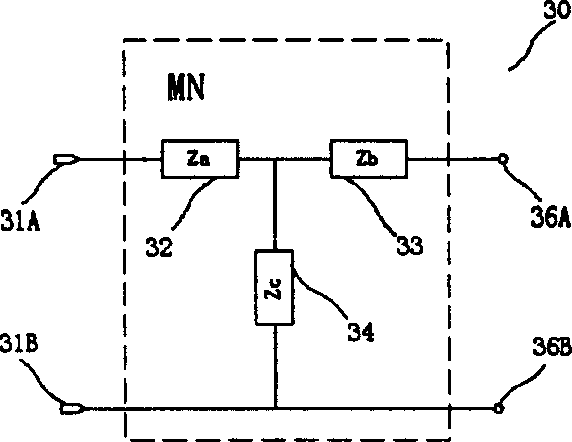
[0095] figure 1 The composition, structure, electrical parameters and their measurement reference points (planes) of the prototype circuits used in this paper are described. The amplifying circuit as a whole is composed of an input matching network (16), a transistor active circuit part (17), and an output matching network (18) in cascaded combination. It should be noted that the component topology of 16 and 18 is shown as figure 1 form, specific circuit specifications and topological forms are in image 3 Figure 4 And it will be described in detail in the text of the present invention. One of the key points of the present invention lies in the calculation method and selection method of these topological structures.

[0096] What needs special a...


PUM


Abstract

Improving efficiency of designing circuits and reducing complexity for match between input and output networks is realized through Pi type or T type network or degraded Pi type or T type network. Transition matrix is utilized to describe and calculate optimal input and output networks of amplification circuit. Active circuit unit containing transistor in negative feedback is described and calculated through scattering matrix, which then transformed to transition matrix and scattering matrix for integral amplification circuit. Standing wave ratio of input and output, gain, noise temperature and stability coefficient are calculated and optimized through scattering matrix for integral amplification circuit. Advantages of precision, high efficiency and convenience of the method is proved by execution of computer.

Description

technical field [0001] An optimization design method for microwave amplifying circuits belongs to the technical field of design and optimization of microwave amplifying circuits. Background of the invention [0002] The development of modern mobile communication has gone through the development from analog system to digital system, and the digital mobile communication system has also experienced the evolution of frequency division multiplexing (FDMA), time division multiplexing (TDMA) to code division multiple access (CDMA) wireless communication. The CDMA method can achieve the signal-to-noise ratio in exchange for a more effective bandwidth. That is to say, improving the signal-to-noise ratio of the receiving system is equivalent to increasing the number of users, so the research on amplifier LNA and front-end system with low noise figure is one of the key research points in the field of microwave communication circuit. Communication LNAs must meet special requirements, s...

Claims


Application Information

Patent Timeline
IPC IPC(8): H03F1/56H03F3/189H04B7/00
Inventor 曹必松高飞张晓平郜龙马高葆新
Owner TSINGHUA UNIV
Learn More