
Double pad oxide technique for processing shallow trench isolation

A shallow trench isolation and oxide technology, which is applied in the direction of electrical components, semiconductor/solid-state device manufacturing, circuits, etc., can solve the problems that the pad oxide thickness should not be too thick, the pad oxide should not be too thin, and rough

Inactive Publication Date: 2005-01-26
SEMICON MFG INT (SHANGHAI) CORP +1
View PDF0 Cites 0 Cited by
  • Summary
  • Abstract
  • Description
  • Claims
  • Application Information

AI Technical Summary

Problems solved by technology

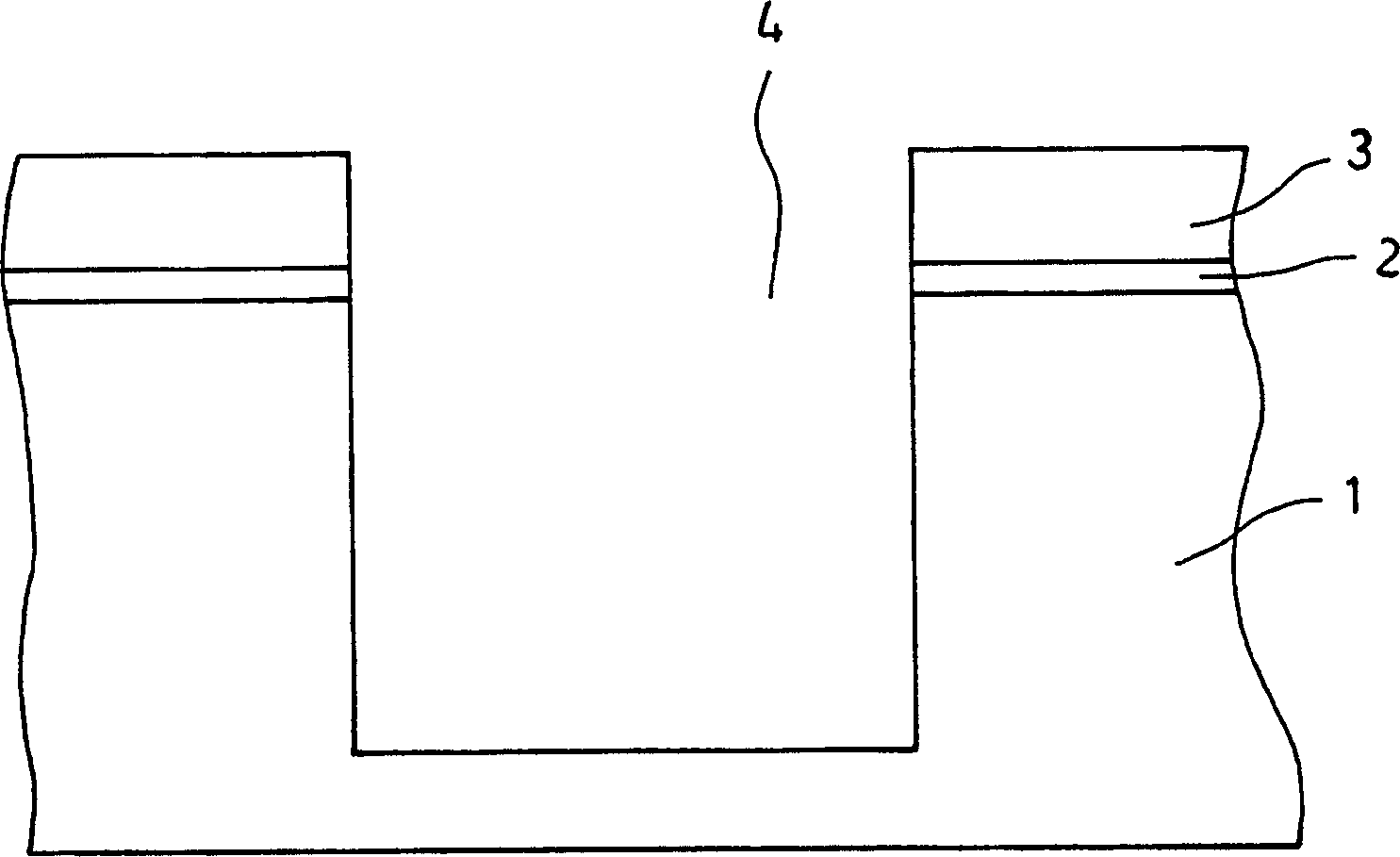
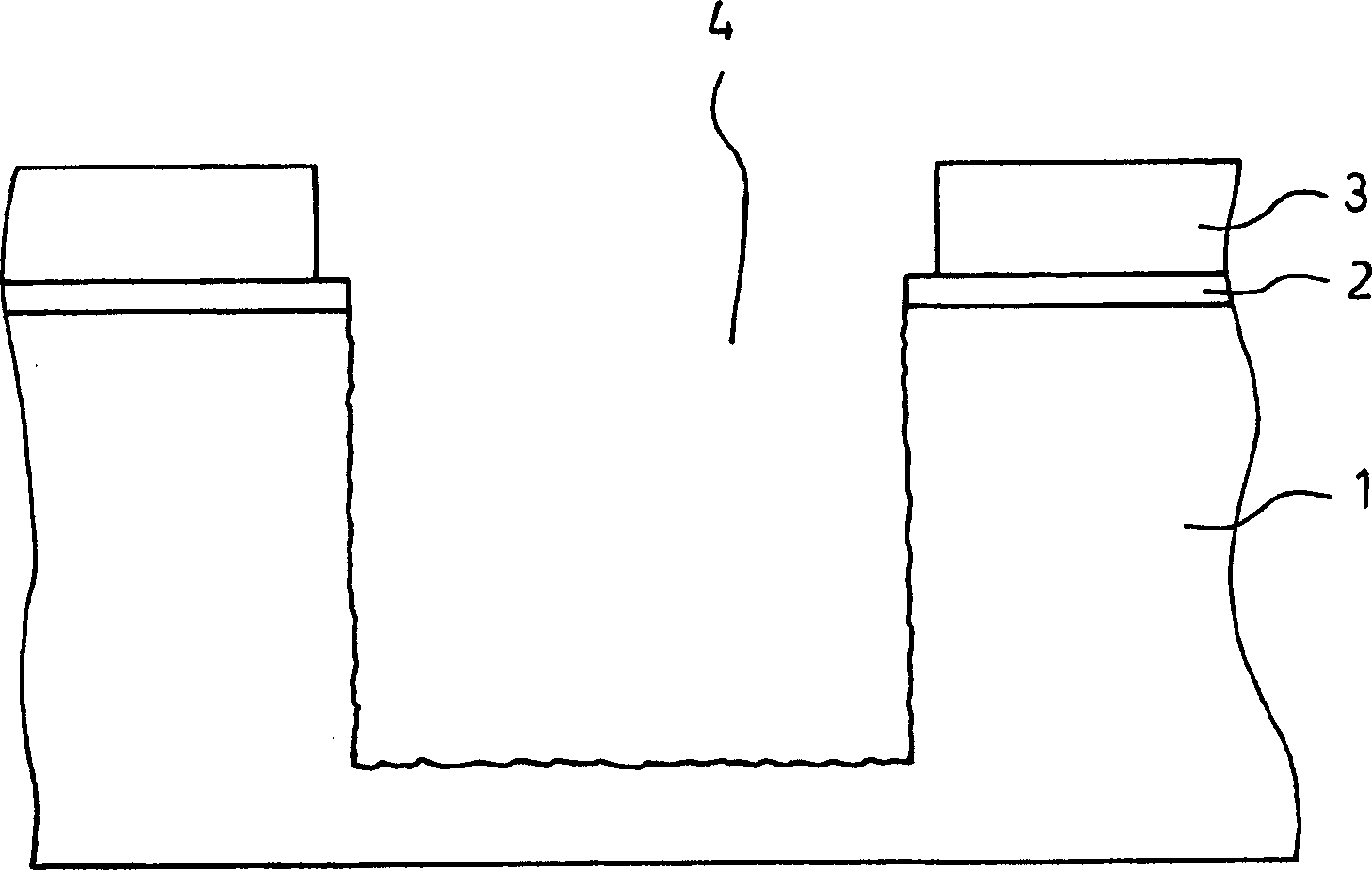
[0004] In the above-mentioned known shallow trench isolation process, since the pad oxide 5 is deposited after the nitride 3 is etched back, the thickness of the pad oxide cannot be too thick to reserve more space for the next step. A trench oxide fill without the liner oxide thickness being too thin to provide corner rounding
Therefore, the thickness selection range of the pad oxide 5 is strictly limited
[0005] In addition, since the pad oxide 5 is deposited after the nitride 3 is etched back, the sidewalls of the shallow trench 4 are caused by H 3 PO 4 etch and become quite rough (eg figure 2 shown), so it also has a negative impact on the isolation effect of the shallow trench 4

Method used


Image

  • Double pad oxide technique for processing shallow trench isolation
  • Double pad oxide technique for processing shallow trench isolation
  • Double pad oxide technique for processing shallow trench isolation

Examples


Embodiment Construction

[0025] Preferred embodiments of the present invention are described below with reference to the accompanying drawings.

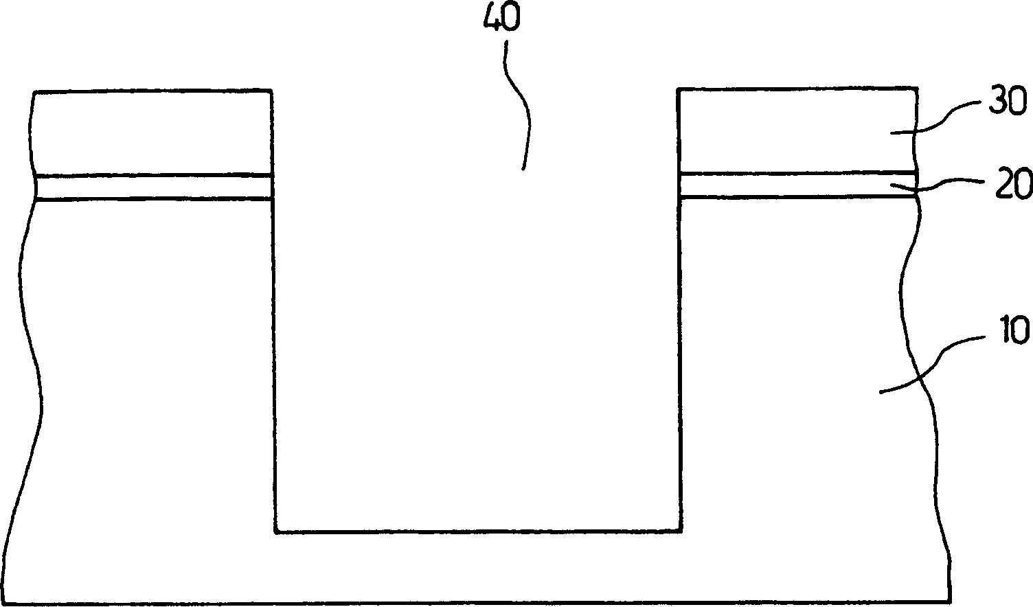
[0026] first reference image 3 , a silicon dioxide layer 20 and a silicon nitride layer 30 are sequentially deposited on the silicon substrate 10 . The thickness of the silicon dioxide layer 30 is about 20 to 60 nm, and it is used to relieve the stress between the silicon substrate 10 and the silicon nitride layer 30 . The thickness of the silicon nitride layer 30 is about 150 to 200 nm, and the pattern on the photomask is transferred through lithography and etching processes, so as to be used as a mask when forming shallow trenches. In addition, the silicon nitride layer 30 can also be used as a stop layer for chemical mechanical polishing (CMP). Then, lithography and etching processes are carried out to form such as figure 1 Shallow trenches 40 are shown.

[0027] After forming the shallow trench 40, the reference Figure 4 , depositing a first pad o...


PUM

PropertyMeasurementUnit
depthaaaaaaaaaa
thicknessaaaaaaaaaa
thicknessaaaaaaaaaa

Abstract

The invention provides a shallow-channel isolated double-pad oxide technique, containing: depositing and forming silicon oxide layer and silicon nitride layer on a silicon substrate, and then etching to form a shallow channel; depositing a first pad oxide on the surface of the shallow channel; etching the nitride layer with H3PO4; removing the first pad oxide by wet-etching; and depositing a second pad oxide on the surface of the shallow channel.

Description

technical field [0001] The invention relates to a shallow trench isolation process method in a semiconductor element, in particular to a shallow trench isolation process utilizing double pad oxides. Background technique [0002] With the continuous improvement of the integration degree of the semiconductor device, the process of the semiconductor device must also be updated according to the situation. For example, in a micron process, field oxides used for isolation purposes need to occupy a large area when used in a deep sub-micron process (below 0.25 μm), and will affect the planarity of the device. In addition, when the field oxide is formed, the bird's beak effect will inevitably occur. However, no matter how the process of the field oxide is changed, it is difficult to control the length of both sides of the bird's beak to less than 1 μm. The result will affect the accuracy of the process. Therefore, shallow trench isolation (STI) technology is generally used as the m...

Claims


Application Information

Patent Timeline
Patent Type & Authority Applications(China)
IPC IPC(8): H01L21/31H01L21/469
Inventor 尹德源
Owner SEMICON MFG INT (SHANGHAI) CORP
Learn More