A process for manufacturing a 0.15-micron T-shaped grid

A production method and process technology, which is applied in the field of 0.15 micron T-shaped gate process, can solve the problems of long production cycle and low precision, and achieve the effects of saving time, improving work efficiency, and not affecting the isolation effect

Active Publication Date: 2021-09-28
CHENGDU HIWAFER SEMICON CO LTD
View PDF3 Cites 0 Cited by
  • Summary
  • Abstract
  • Description
  • Claims
  • Application Information

AI Technical Summary

Problems solved by technology

[0004] The purpose of the present invention is to overcome the problems of long production cycle and low precision in the production of 0.15 micron T-shaped grid in the prior art, and provide a process manufacturing method of 0.15 micron T-shaped grid

Method used


Image

  • A process for manufacturing a 0.15-micron T-shaped grid
  • A process for manufacturing a 0.15-micron T-shaped grid
  • A process for manufacturing a 0.15-micron T-shaped grid

Examples


Embodiment 1

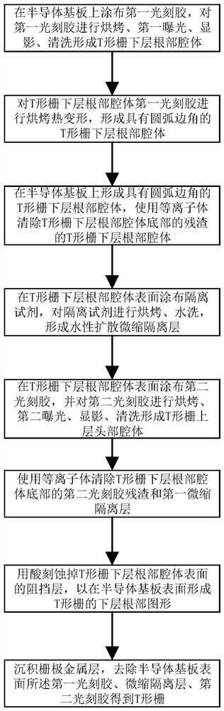
[0047] like figure 1 Shown, in embodiment 1, a kind of process manufacturing method of 0.15 micron T-shaped gate, the method specifically comprises the following steps:

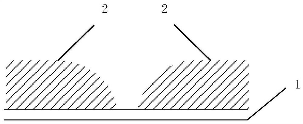
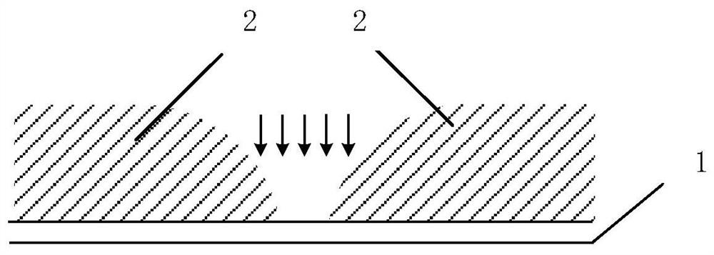
[0048] S01: Form a T-shaped grid lower root cavity with arc corners on the semiconductor substrate 1, and use plasma to remove the residue at the bottom of the T-shaped grid lower root cavity; specifically, as figure 2As shown, the characteristic size of the lower root cavity of the T-shaped gate with rounded corners is smaller than the target characteristic size of 0.15 μm, and the characteristic size of the lower root cavity of the T-shaped gate is that the lower root cavity on both sides of the T-shaped gate is in contact with the semiconductor substrate. The relative distance of the position; such as image 3 As shown, the plasma used is O2 plasma, and the flow rate of O2 plasma is controlled at 1-4Torr, and the power is controlled at 10-170W, which can clean the residue at the bottom of the root cavity...

Embodiment 2

[0056] This embodiment has the same inventive idea as Embodiment 1, and this embodiment is a further optimization based on Embodiment 1. Specifically, this embodiment provides a process for manufacturing a 0.15-micron T-shaped grid. The method is specific Include the following steps:

[0057] S11: Form a T-shaped grid lower root cavity with rounded corners on the semiconductor substrate 1, and use plasma to remove residues at the bottom of the T-shaped grid lower root cavity; wherein, the T-shaped lower root cavity with rounded corners The characteristic size of the cavity is smaller than the target characteristic size of 0.15 μm, and the characteristic size of the lower root cavity of the T-shaped grid is the relative distance between the lower root cavity on both sides of the T-shaped grid and the contact position of the semiconductor substrate; the plasma is O2 plasma, and the The O2 plasma flow rate is controlled at 1-4Torr, and the power is controlled at 10-170W, which ca...


PUM

PropertyMeasurementUnit
sizeaaaaaaaaaa
lengthaaaaaaaaaa
thicknessaaaaaaaaaa

Abstract

The invention discloses a process manufacturing method of a 0.15-micron T-shaped grid, which belongs to the technical field of semiconductor manufacturing technology. Remove the residue at the bottom of the root cavity of the lower layer of the T-shaped grid; apply an isolation reagent on the surface of the root cavity of the lower layer of the T-shaped grid, bake and wash the isolation reagent to form a water-based diffusion miniature isolation layer; prepare the head cavity of the upper layer of the T-shaped grid Body, using plasma to remove the second photoresist residue and the first micro-isolation layer at the bottom of the bottom root cavity of the T-shaped grid; using acid to etch the barrier layer on the surface of the lower root cavity of the T-shaped grid; depositing the gate metal layer , removing all the photoresist on the surface of the semiconductor substrate to obtain a T-shaped gate. The invention needs two photolithography processes to complete the fabrication of the 0.15-micron T-shaped grid, which greatly saves time, improves work efficiency, and facilitates mass production.

Description

technical field [0001] The invention relates to the technical field of semiconductor manufacturing technology, in particular to a manufacturing method of a 0.15-micron T-shaped gate. Background technique [0002] Today, high electron mobility transistors (High Electron Mobility Transistor, referred to as HEMT devices) have become the preferred technology for next-generation RF / microwave power amplifiers. Among them, gate fabrication is the most difficult in the semiconductor process that affects the performance of HEMT devices. In order to increase the operating frequency of the device, the gate length must be continuously reduced. At present, the gate length has reached the sub-micron or even nanometer level, but the reduction of the gate length will bring other problems, mainly the increase of the gate resistance. Therefore, it is necessary to make a T-shaped gate to reduce the parasitic resistance of the gate. transistor noise. [0003] At present, there are two ways to...

Claims


Application Information

Patent Timeline
Patent Type & Authority Patents(China)
IPC IPC(8): H01L21/28H01L21/027H01L29/778H01L21/335
CPCH01L21/027H01L21/28008H01L29/66462H01L29/7782
Inventor 毛江敏彭挺陈俊奇郭盼盼
Owner CHENGDU HIWAFER SEMICON CO LTD
Why Eureka
Try Eureka