
Balanced transconductor and electronic device

A balanced, transconductance technology, applied in amplifiers, electrical components, amplifiers with semiconductor devices/discharge tubes, etc., can solve the problems of loop instability, instability, performance loss, etc., to improve the common mode rejection ratio, The effect of improving stability

Inactive Publication Date: 2005-02-02
NXP BV
View PDF0 Cites 0 Cited by
  • Summary
  • Abstract
  • Description
  • Claims
  • Application Information

AI Technical Summary

Problems solved by technology

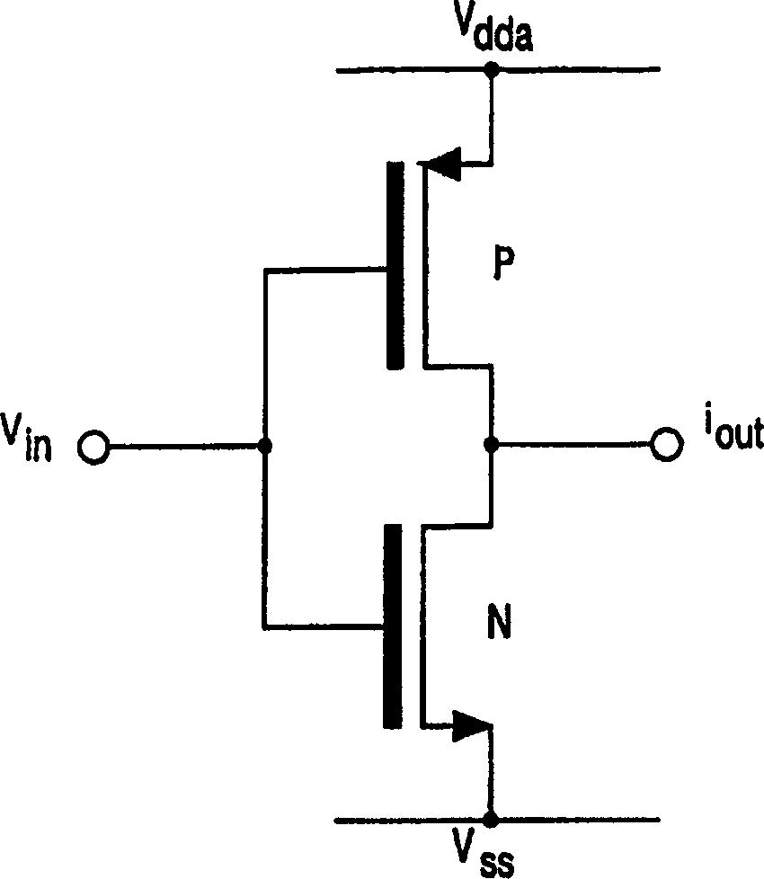
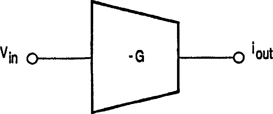
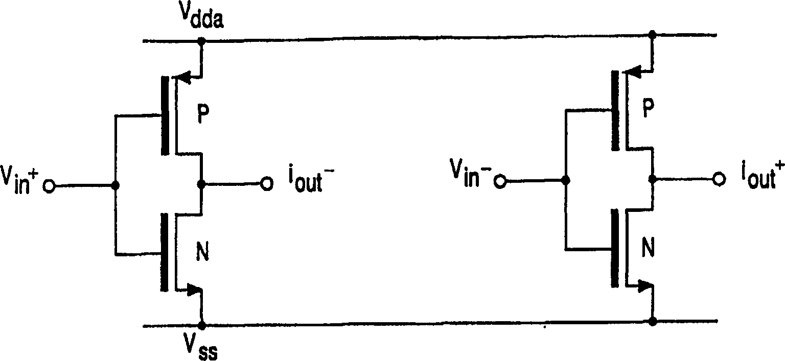
However, including both this structure and image 3 A loop with a simple balanced transconductance in the
use Figure 7 A purpose-made filter of balanced transconductance will dissipate the image 3 A filter made of simple balanced transconductance (although this filter is unstable) 3 times the power, which is a big performance loss
and, Figure 7 The common mode rejection of the balanced transconductance is only 0.5(6dB)

Method used


Image

  • Balanced transconductor and electronic device
  • Balanced transconductor and electronic device
  • Balanced transconductor and electronic device

Examples


Embodiment Construction

[0030] Reference is made to 10, which shows a balanced transconductance 100 having first and second inputs 10, 15, first and second outputs 20, 25, and first and second primary single-ended transconductances 30, 35 each having a transconductance -G and are coupled with the supply currents of the first and second outputs 20, 25, respectively. A common mode feedback cancellation network 200 is coupled between the first and second inputs 10 , 15 of the balanced transconductor 100 and the inputs 40 , 45 of the first and second primary single-ended transconductors 30 , 35 .

[0031] The cancellation network 200 includes a first resistor 50 of resistance R coupled between the first input 10 of the balanced transconductance 100 and the input 40 of the first primary single-ended transconductance 40, and a resistance of R A second resistor 55 coupled between the second input 15 of the balanced transconductance 100 and the input 45 of the second primary single-ended transconductor 45 . ...


PUM


Abstract

A balanced transconductor having a pair of voltage inputs and a pair of current outputs comprises a pair of single-ended transconductors, one in each signal path and a cancellation network. The cancellation network cancels at the inputs to the single-ended transconductors a common mode voltage appearing at the voltage inputs so that no common mode output current results. The cancellation network may comprise four half-size single-ended transconductors drawing half the supply current of full-size single-ended transconductors.

Description

technical field [0001] The present invention relates to a balanced transconductance suitable for use in an active electronic filter and an electronic device comprising the balanced transconductance. Background technique [0002] In the field of wireless communications, the preferred wireless receiver architecture for obtaining a highly sensitive, fully integrated wireless transceiver is a low IF (intermediate frequency) polyphase receiver architecture. A key to the success of this polyphase architecture is the ability to integrate channel filters. In order to increase the level of circuit integration and reduce power consumption, it is desirable to implement wireless transceivers with mixed analog and digital integrated circuits (ICs), and it is desirable to implement such mixed-signal ICs in a low-voltage digital CMOS process. [0003] One component that can be used to implement an integrated channel filter is a transconductance. Transconductance is an important component...

Claims


Application Information

Patent Timeline
IPC IPC(8): H03F3/34H03F3/45H03H11/04H03H11/12
CPCH03F2200/294H03H2011/0494H03F3/45991H03F2200/372H03H11/045H03F3/45959
Inventor J·B·胡赫斯
Owner NXP BV
Learn More