Wiring pattern check up apparatus

A wiring pattern and inspection device technology, applied in the direction of measuring devices, optical devices, underwater structures, etc., can solve the problems of difficult wiring pattern inspection, unclear, false detection of attached dust, etc., to shorten the inspection the effect of time

Inactive Publication Date: 2005-02-09
USHIO DENKI KK
View PDF1 Cites 9 Cited by
  • Summary
  • Abstract
  • Description
  • Claims
  • Application Information

AI Technical Summary

Problems solved by technology

[0033] As described above, it is difficult to inspect the thickness of the wiring pattern by only inspecting by reflected illumination light or inspection by transmitted illumination light, and it is impossible to detect false inspections caused by adhering dust.
[0034] As described in the above-mentioned Patent Document 1, if reflected light and tr

Method used


Image

  • Wiring pattern check up apparatus
  • Wiring pattern check up apparatus
  • Wiring pattern check up apparatus

Examples


Embodiment Construction

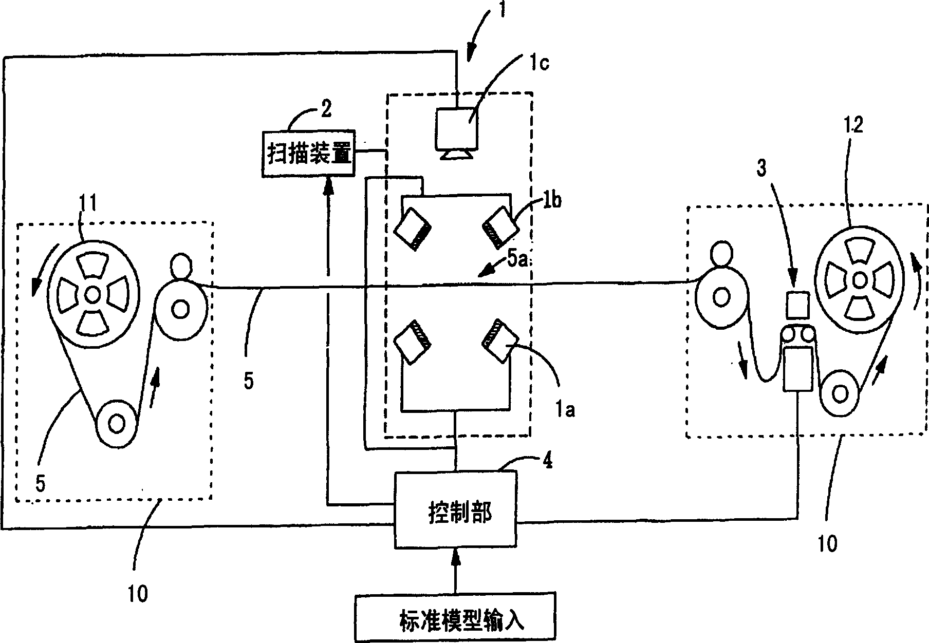
[0057] figure 1 is a block diagram showing a wiring pattern inspection device according to an embodiment of the present invention.

[0058] In addition, in the following examples, the case where the substrate is a TAB tape will be described, but the present invention can also be applied to inspection of various substrates using transmitted illumination light other than the TAB tape.

[0059] The graphic inspection device of the present embodiment, as shown in this figure, has: the tape conveying mechanism 10 that is constituted by the output reel 11 of conveying TAB tape 5 or take-up reel 12 etc.; The belt 5 irradiates transmitted illumination light and reflected illumination light, and captures the pattern 5a; the scanning device 2 scans the inspection part 1 on the upper part of the inspection pattern 5a of the TAB tape; the marking part 3 attaches a mark to the unqualified pattern.

[0060] In the marking part 3, the pattern judged as defective may be punched with a punch...


PUM


Abstract

Provided is an inspection apparatus of a wiring pattern that has a small number of false detections and can reduce inspection time by combining an inspection by vertical illumination and that by reflection illumination. A pattern 5a on a TAB tape 5 is carried to an inspection section 1 by a tape conveyance mechanism 10, illumination light is applied from a transmission illumination means 1a, the transmitted illumination image of the pattern 5a is imaged by a CCD line sensor 1c, illumination light is applied from a vertical illumination means 1b, and the vertical illumination image from the pattern 5a is imaged. The captured image is sent to a control section 4. The control section 4 compares the pattern of the transmission illumination image with a first reference pattern, inspects the pattern 5a, compares the pattern of the vertical illumination image at a position corresponding to a faulty section with a second reference pattern regarding the pattern 5a that is determined to be a faulty candidate, and determines whether the pattern 5a is conforming or not.

Description

technical field [0001] The present invention relates to a wiring pattern inspection device which irradiates a tape-loaded TAB (TapeAutomated Bonding) tape with illumination light, uses an imaging device to pick up the wiring pattern formed on the TAB tape, and compares it with a standard pattern to automatically perform an appearance inspection. . Background technique [0002] In order to meet the requirements of high integration and high-density assembly, semiconductor devices are advancing multi-lead and miniaturization. In order to facilitate the increase in number of leads and miniaturization, a method of connecting a semiconductor chip to a plurality of leads provided on a film-shaped TAB tape is employed. [0003] Figure 5 Indicates the order in which TAB tapes are made. [0004] Such as Figure 5 As shown in (a), the TAB tape 101 is on a resin film 102 with a thickness of about 20 to 150 μm (mostly 25 to 75 μm) and a width of about 35 to 165 μm. The adhesive 104 h...

Claims


Application Information

Patent Timeline
IPC IPC(8): G01B11/24G01N21/956H01L21/60
CPCE02D29/025E02D29/0266E02D2600/20
Inventor 笹部高史永森进一
Owner USHIO DENKI KK
Why Eureka
Try Eureka