Method and apparatus for analyzing the state of generation of foreign particles in semiconductor fabrication process

a technology of foreign particles and semiconductor fabrication, which is applied in the direction of semiconductor/solid-state device testing/measurement, optical radiation measurement, instruments, etc., can solve the problems of failure to increase the inspection frequency up to a sufficient value, the defect of wiring and short-circuits, and the breakdown of the insulating film, etc., to achieve the effect of improving the yield, increasing the number of defects generated, and improving the yield

Inactive Publication Date: 2005-09-22
RENESAS ELECTRONICS CORP
View PDF5 Cites 14 Cited by
  • Summary
  • Abstract
  • Description
  • Claims
  • Application Information

AI Technical Summary

Benefits of technology

[0015] At the time of starting of mass production in a semiconductor fabrication process, each process and equipment are evaluated by means of an evaluation equipment of high performance which is expensive, for making evaluation and debug of material, process, apparatus and design, and at the time of mass production, the number of processes and equipment in the production line are minimized, particularly the number of inspection and evaluation items is decreased to reduce the equipment cost and shorten the time required for inspection and evaluation. To this end, various considerations are given to permit a smooth and quick evaluation at the time of starting of mass production. For example, sampling is made along this line or a semiconductor substrate is inspected using an improved foreign particle detecting and analyzing system to clear up the cause of generation of foreign particles, then the specification of inspection in the acquisition of materials is changed or a certain measure is taken against a dust generation source on the basis of the result obtained, which result is fed back to each material, process and apparatus to, for example, change the specification of a dust-prone process into a design of elements which strong against the generation of dust. At the same time, such result is utilized in preparing specifications for inspection and evaluation in the mass production line, and where required, a monitor for foreign particles on a semiconductor substrate is mounted in a place where foreign particles are apt to occur, or a specification is prepared to monitor only increase and decrease of specific foreign particles present in a specific place.
[0016] By thus separating the mass production starting line and the mass production line from each other, it is made possible to effect an efficient operation of the apparatus for detecting, analyzing and evaluation foreign particles at the time of starting of mass production and hence it is possible to perform the mass production starting work rapidly. Besides, the reduction in weight of the mass production line can be attained by using a minimum required number of monitoring apparatus of a simple structure as the foreign particle inspecting and evaluating apparatus used in the mass production line.
[0017] In connection with the above monitoring apparatus used in the mass production line according to the present invention, we have paid attention to the following method in order to realize, using the existing technique, a small-sized, high-speed inspection apparatus having an equal function to that of the conventional large-sized apparatus. First, the repeatability of memory was noted. Heretofore, a method of removing repetitive patterns and detecting defects has been known. This conventional method ensures a detection performance. However, no convenient point has been referred to about such method in realizing the said monitoring apparatus. Further, it is not necessary to monitor all of points on a semiconductor substrate, but it suffices to monitor the upper surface of the substrate at a certain specific ratio. In the manufacture of a memory having lots of repetitive patterns, even a mere monitor of only the repetitive portion of the memory is very effective.
[0018] In repetitive patterns, the radiation of a coherent light causes exit of light only in a certain specific direction. More particularly, in the case of memory, light emerging in a specific direction from a repetitive portion can be intercepted using a spatial filter and it is possible to detect, in high sensitivity, foreign particles which are not apt to occur repeatedly. In this case, if liquid crystal is used as the spatial filter, the shape of the spatial filter can be changed as desired by turning on-off of the liquid crystal and therefore it is possible to inspect any repetitive pattern automatically.
[0019] The reason why the yield in semiconductor fabrication is improved by the above means is as follows. As a result of a strict experiment for detecting the number of foreign particles on a semiconductor substrate, it turned out that the number of foreign particles increased or decreased suddenly, not gradually. Heretofore, since the number of foreign particles has been considered to increase or decrease gradually, the inspection of foreign particles has been conducted at a frequency of one lot or one sheet a day as noted previously. In such a low inspection frequency, however, a sudden increase in the number of foreign particles will be overlooked, or detection may be made in a little while after the increase, thus resulting in occurrence of a considerable number of defects. That is, in the mass production line, it is necessary to detect the generation of foreign particles and take a countermeasure as soon as possible. With the lapse of time from the generation of foreign particles until detection thereof, the number of defects generated increases and the yield lowers. In other words, a high yield can be ensured by shortening the time elapsed from the time when foreign particles are generated until when the generation is detected. That is, the effect of the foreign particle inspection can be exhibited to the maximum extent by shortening the sampling time in monitor or ideally by sampling in real time.
[0020] In the conventional apparatus, moreover, a semiconductor substrate is pulled out for inspection and in this case foreign particles will newly be deposited on the semiconductor substrate, thus also resulting in lowering of the yield. On the other hand, the foreign particle inspection apparatus according to the present invention permits the inspection without the need of pulling out a semiconductor substrate, so that there will be no lowering of the yield caused by the deposition of foreign particles on the substrate.

Problems solved by technology

In the conventional semiconductor fabrication process, if foreign particles are present on a semiconductor substrate (wafer), they will cause defects such as defective insulation of wiring and short-circuit.
Further, in the case where a fine foreign particle is present in a semiconductor substrate provided with very fine semiconductor elements, such foreign particle will cause breakdown of an insulating film of a capacitor or a gate oxide film.
Thus, it takes time for conveyance of the semiconductor substrate and for the inspection of foreign particles, so that it is difficult to increase the inspection frequency up to a sufficient value.
In the prior art, in addition to the large scale of equipment, a long time is required for the inspection, so for realizing a real-time monitor using such conventional apparatus, it is necessary to arrange a large number of large-sized apparatus, but actually this has been difficult.
Such inspection in the prior art has been remote from the ideal real-time sampling in the mass production line.
As time elapses from the generation of foreign particles up to the detection thereof, the number of defects generated increases and hence the yield lowers.

Method used


Image

  • Method and apparatus for analyzing the state of generation of foreign particles in semiconductor fabrication process
  • Method and apparatus for analyzing the state of generation of foreign particles in semiconductor fabrication process
  • Method and apparatus for analyzing the state of generation of foreign particles in semiconductor fabrication process

Examples


Embodiment Construction

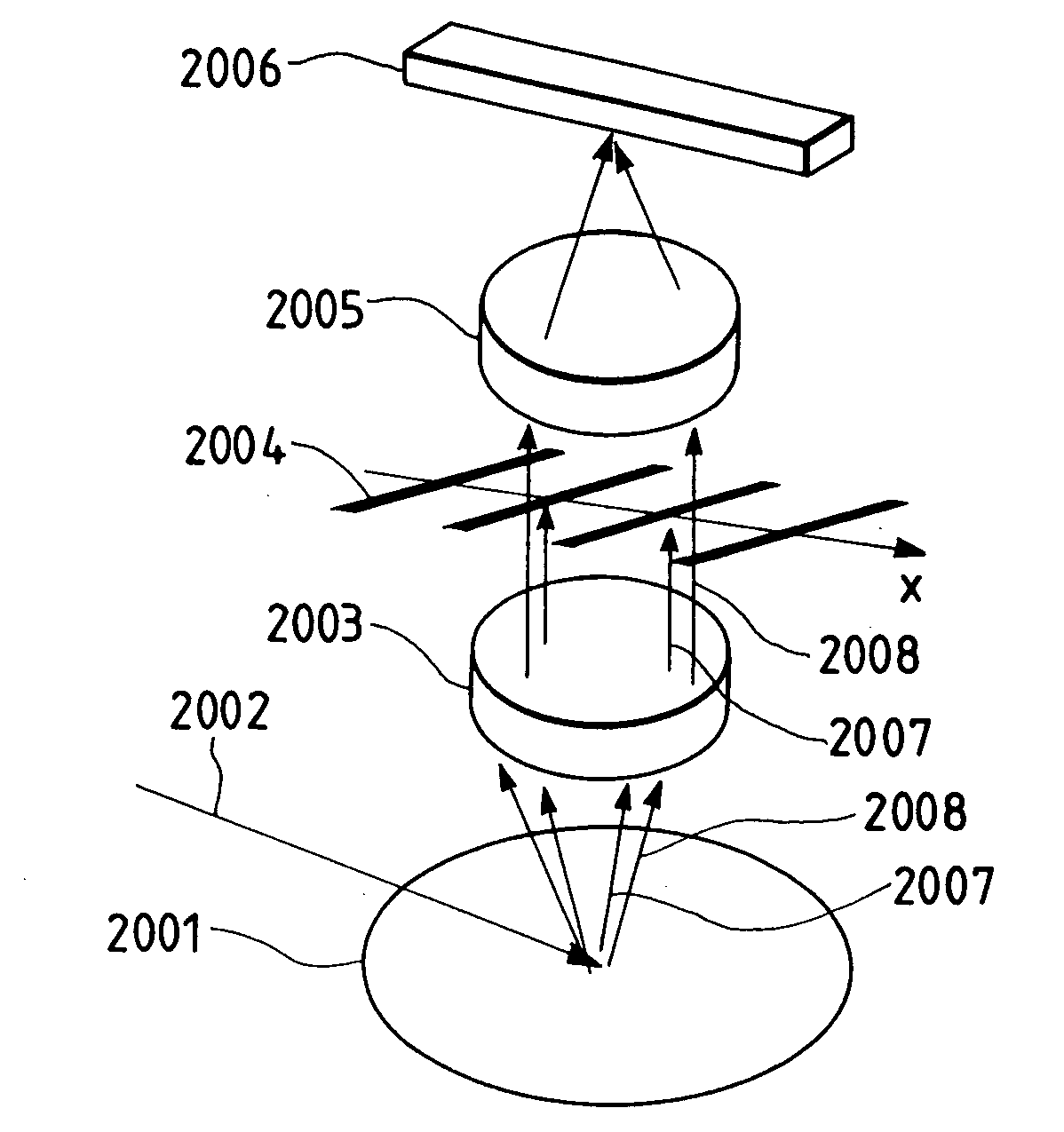
[0064] The present invention is an improvement over U.S. Ser. No. 07 / 778,363 and therefore the contents described in the U.S. Ser. No. 07 / 778,363 will here be omitted.

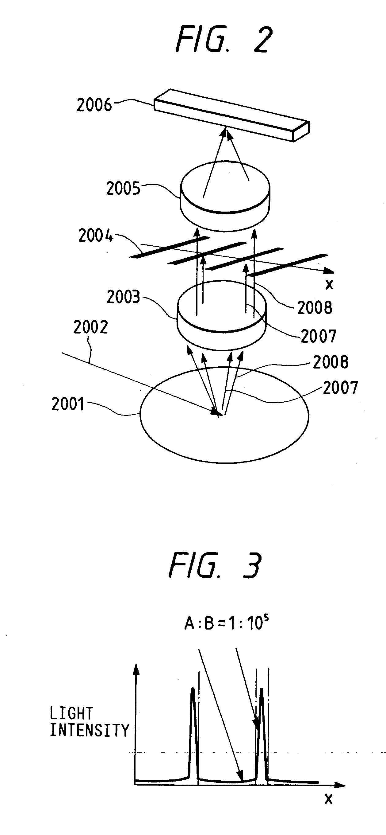
[0065] In realizing a small-sized, high-speed, foreign particle inspection apparatus, the method using a spatial filter is more suitable than the polarized light detection method shown in the prior art (Japanese Patent Laid Open No. 89336 / 87). The reason for this conclusion will be stated below with reference to FIGS. 1, 2 and 3.

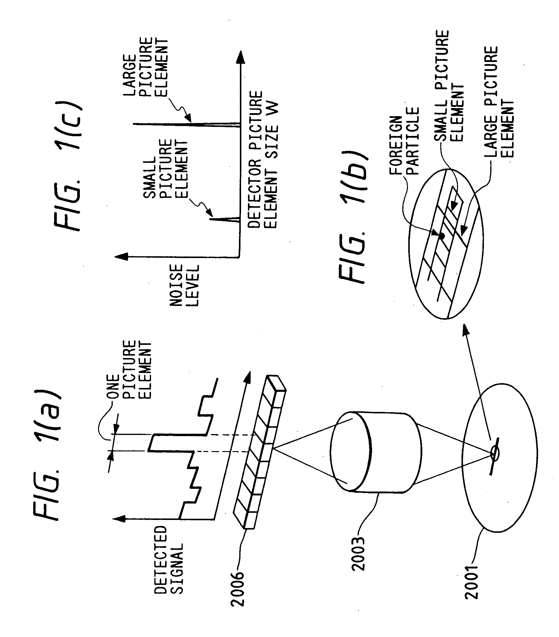
[0066] In the method wherein light is radiated to a sample and scattered light from foreign particles is detected in the scattered light from patterns formed on the sample surface causes noise. The larger the size of a picture element (a minimum unit detected as one signal) in a detector 2006, the larger the said noise, as shown in FIG. 1(c). Since the patterns as a noise source are formed substantially on the whole surface of the sample, the noise becomes larger in proportion to the picture ...


PUM

PropertyMeasurementUnit
sizeaaaaaaaaaa
sizeaaaaaaaaaa
clock frequencyaaaaaaaaaa

Abstract

An apparatus and method for detecting defects on a specimen includes an illumination optical unit which obliquely projects a laser onto a region which is longer in one direction on a surface of a specimen than in a transverse direction, a table unit which mounts the specimen and which is movable, a detection optical unit which detects light from the specimen illuminated by the laser with an image sensor while the table is moving, and a signal processor. The signal processor processes a signal outputted from the image sensor of the detection optical unit and converted to a digital signal and extracts defects of the specimen by comparing the converted digital signal with a reference digital signal. A display unit displays information of defects extracted by the signal processor.

Description

CROSS-REFERENCE TO RELATED APPLICATIONS [0001] This application is a continuation application of U.S. application Ser. No. 09 / 805,188, filed Mar. 14, 2001, which is a continuation application of U.S. application Ser. No. 08 / 535,577, filed Sep. 28, 1995, which is a continuation application of U.S. application Ser. No. 08 / 046,720, filed Apr. 16, 1993, now U.S. Pat. No. 5,463,459, which is a continuation-in-part of U.S. application Ser. No. 07 / 679,313, filed Apr. 2,1991, now U.S. Pat. No. 5,233,191 and U.S. application Ser. No. 07 / 778,363, filed Oct. 17, 1991, now U.S. Pat. No. 5,274,434.BACKGROUND OF THE INVENTION [0002] The present invention relates to a method and apparatus for analyzing the state of generation of foreign particles in a semiconductor fabrication process, more particularly, detecting and analyzing foreign particles generated in a mass production starting line and a mass production line of the said process and taking an appropriate countermeasure, or a foreign particl...

Claims


Application Information

Patent Timeline
Patent Type & Authority Applications(United States)
IPC IPC(8): G01N21/00G01N21/94G01N21/95G01N21/956G01R31/308H01J37/00H01L21/00H01L21/66H01L21/68
CPCB82Y15/00G01N21/94G01N21/9501G01N21/95623G01N2021/8822G01R31/308H01L22/12H01J2237/022H01J2237/0225H01L21/67253H01L21/67288H01L21/681H01J37/00
Inventor MORIOKA, HIROSHINOGUCHI, MINORIOHSHIMA, YOSHIMASAKEMBO, YUKIONISHIYAMA, HIDETOSHIMATSUOKA, KAZUHIKOSHIGYO, YOSHIHARU
Owner RENESAS ELECTRONICS CORP
Why Eureka
Try Eureka