Display device
A technology for display devices and display screens, which can be used in identification devices, lighting devices, instruments, etc., and can solve problems such as area reduction
- Summary
- Abstract
- Description
- Claims
- Application Information
AI Technical Summary
Problems solved by technology
Method used
Image
Examples
Deformed example 1
[0095] Below, use Figure 5A , Figure 5B Modification 1 will be described.
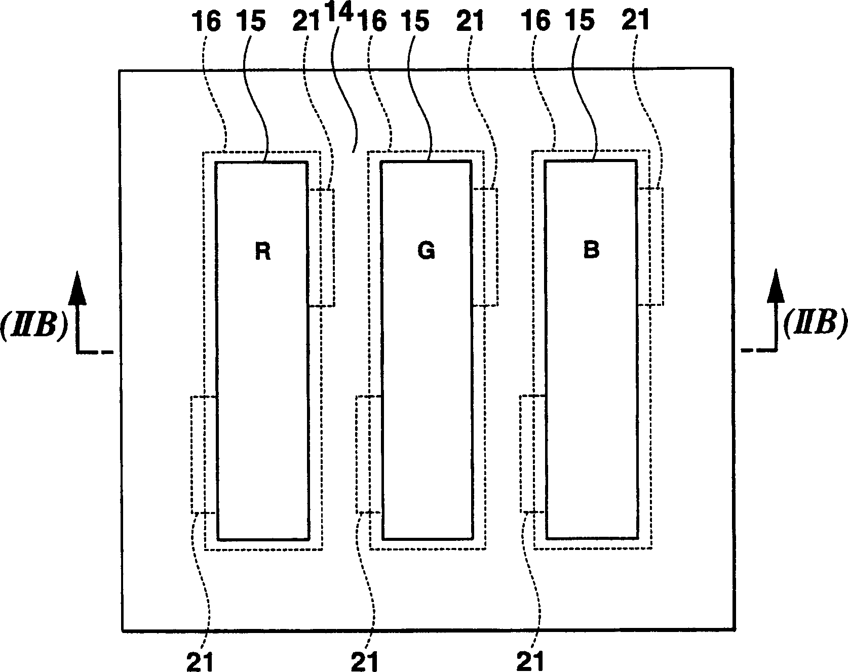
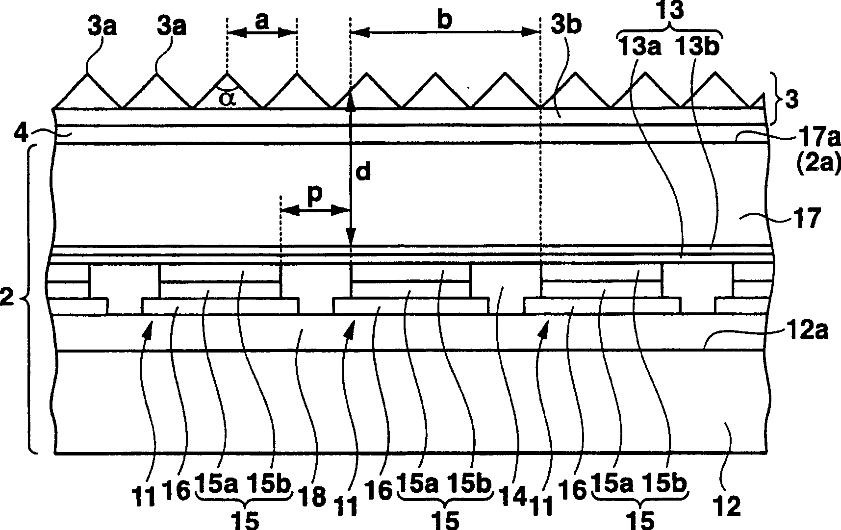
[0096] In the display device of Modification 1, the sealing film 17 is partitioned by the spacer 5 . That is, on the common electrode 13 , the spacer 5 having a mesh shape in plan view is formed corresponding to the insulating film 14 . By forming the separators 5 in a mesh shape in a plan view, a plurality of cells surrounded by the separators 5 are arranged in a matrix. In addition, the EL layer 15 is arranged in each cell when viewed from above. The sealing film 17 is filled in each cell formed by the separator 5 . The film thickness of the spacer 5 is the same as that of the sealing film 17 , and the optical sheet 3 is adhered to the flat surface 2 a formed by the sealing film 17 and the spacer 5 via the optical adhesive 4 . The spacer has better light-shielding performance and the best reflective performance to the light emitted by the EL layer 15 . The display device of Modification 1 has...
Deformed example 2
[0099] Below, use Figure 6A , Figure 6B Modification 2 will be described.
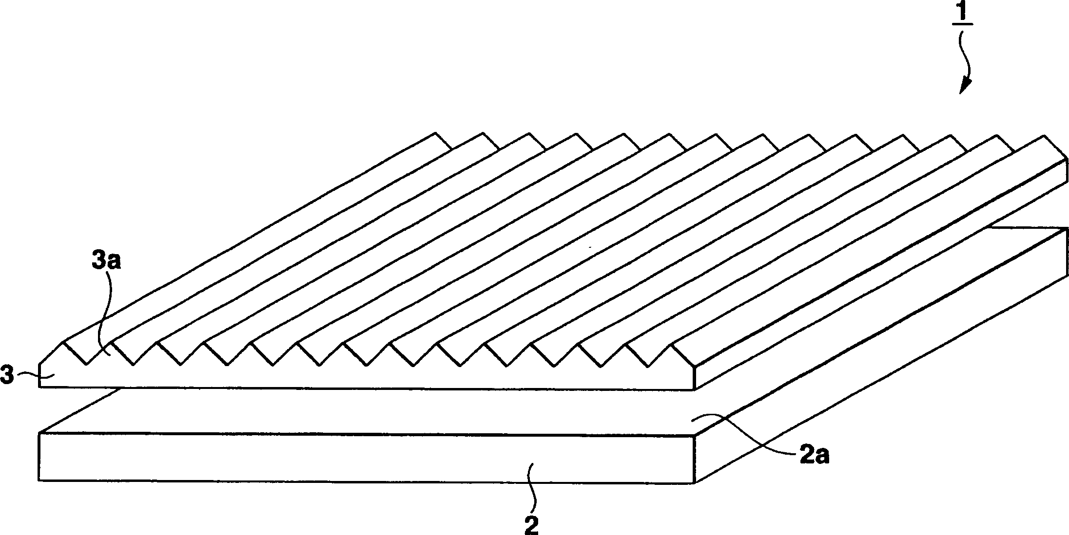
[0100] In the display device of Embodiment 1, the optical sheet 3 is bonded to the surface 2a of the flat panel display 2; and in the display device of Modification 2, such as Figure 6A , Figure 6B As shown, many microprisms 3a are directly formed on the surface 2a of the flat panel display 2 by photolithography. Here, there is an interval between adjacent microprisms 3a, which is the same as the width of the non-light-emitting area between laterally adjacent pixels. In addition, one microprism 3a is arranged opposite to a longitudinal column of pixels. In addition to the above, the display device of Modification 2 is the same as Figure 5A , Figure 5B The display device of Modification 1 shown has the same structure.
Deformed example 3
[0102] Below, use Figure 7A , Figure 8 A, Modification 3 will be described.
[0103] In the display device of Modification 1, there is no space between adjacent microprisms 3a of the optical sheet 3, and one slope of the microprism 3a intersects the other slope of the adjacent microprism 3a. On the other hand, in the display device of Modification 3, if Figure 7A , Figure 7B Shown, there is interval between the adjacent microprisms 3a of optical sheet 3, between adjacent microprisms 3a, form the bottom surface 3b that is roughly parallel with the back side of optical sheet 3, an inclined plane of microprism 3a intersects with bottom surface 3b, Another slope of the adjacent microprism 3a crosses the bottom surface 3b. In addition, one microprism 3 a is arranged opposite to the longitudinal row of pixels, and the bottom surface 3 b is opposite to the spacer 5 . In addition to the above, the display device of Modification 3 is the same as Figure 5A , Figure 5B The d...
PUM
| Property | Measurement | Unit |
|---|---|---|
| Thickness | aaaaa | aaaaa |
Abstract
Description
Claims
Application Information


