Method for dividing disc-like workpiece

A technology for dividing discs and workpieces, applied in electrical components, manufacturing tools, metal processing, etc., can solve problems such as damaged circuits and low-k film peeling

Inactive Publication Date: 2005-02-16
DISCO CORP
View PDF1 Cites 8 Cited by
  • Summary
  • Abstract
  • Description
  • Claims
  • Application Information

AI Technical Summary

Problems solved by technology

Since the groove has a small width, there is a problem that the blade comes into contact with the side of the groove and then the end face of the divided low-k film, so that the low-k film comes off and damages the circuit

Method used


Image

  • Method for dividing disc-like workpiece
  • Method for dividing disc-like workpiece
  • Method for dividing disc-like workpiece

Examples


Embodiment Construction

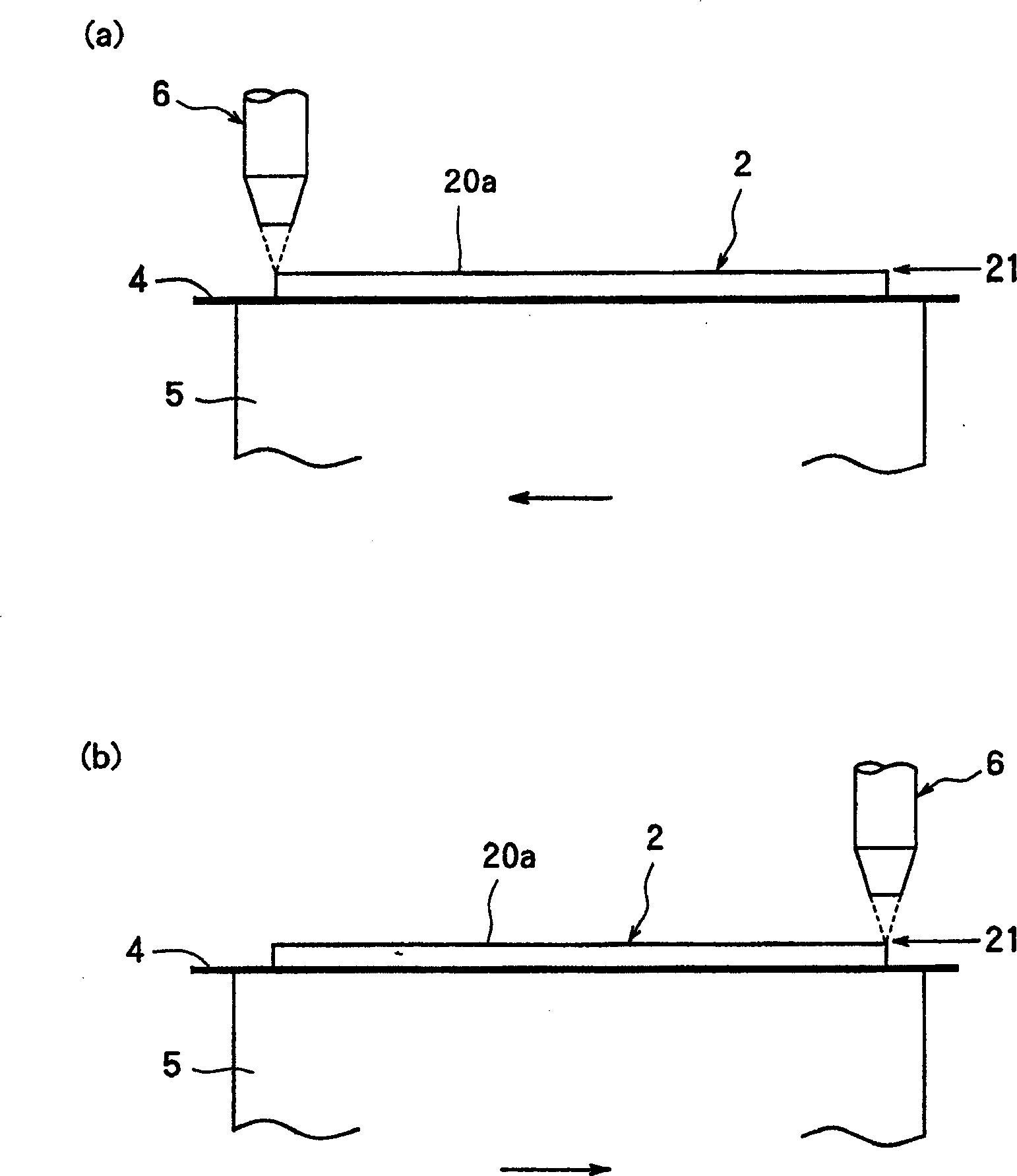
[0022] The method for cutting a disc-shaped workpiece according to the present invention will be described in detail below with reference to the accompanying drawings.

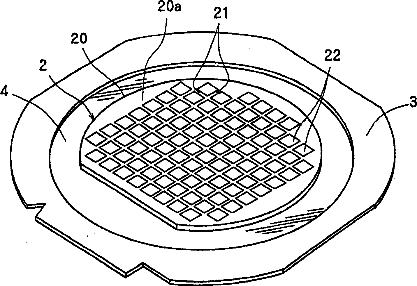
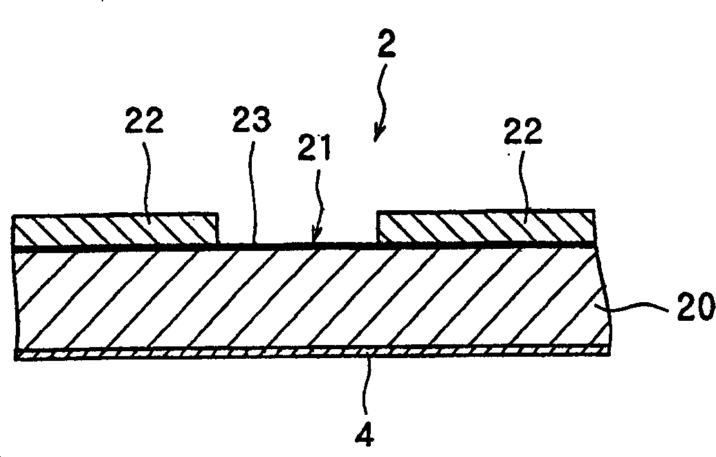
[0023] figure 1 is a perspective view of a semiconductor wafer (as a disk-shaped workpiece) to be divided according to the invention. exist figure 1 In the shown semiconductor wafer 2, a plurality of dividing lines 21 are formed in a lattice pattern on the front surface 20a of a substrate 20 (which is a silicon wafer), and circuits 22 are formed in each of the plurality of regions separated by the plurality of dividing lines 21. formed in. In the illustrated embodiment, as figure 2 As shown, a low-dielectric insulating film (low-k film) 23 composed of an inorganic thin film such as SiOF or BSG (SiOB) and an organic thin film such as a polymer (such as polyimide or parylene) is laminated. On the front side 20 a of the substrate 20 , and the circuit 22 is formed on the front side of the low-k thin film 23 ....


PUM

PropertyMeasurementUnit
wavelengthaaaaaaaaaa
diameteraaaaaaaaaa
thicknessaaaaaaaaaa

Abstract

A method of dividing a plate-like workpiece having a layer that is made of a different material from that of a substrate and is formed on the front surface of the substrate along predetermined dividing lines, comprising a laser beam application step for applying a laser beam along the dividing lines formed on the plate-like workpiece to form a plurality of grooves deeper than the layer and a cutting step for cutting the plate-like workpiece with a cutting blade along the plurality of grooves formed in the laser beam application step, wherein a length between the outer sides of grooves on both sides formed in the laser beam application step is set to be larger than the thickness of the cutting blade and the cutting blade cuts the area between the outer sides of the grooves on both sides in the cutting step.

Description

technical field [0001] The present invention relates to a method of dividing a disk-shaped workpiece, such as a semiconductor wafer or the like. In particular, it relates to a method for dividing a disc-shaped workpiece having a layer made of a different material than the substrate and formed on the front side of the substrate along predetermined dividing lines. Background technique [0002] As is well known to those skilled in the art, in the production process of semiconductor devices, by dividing the plurality of regions by dividing lines called "scribe lines", the dividing lines Individual semiconductor chips are produced by forming circuits such as ICs or LSIs in a lattice pattern on the front surface of a semiconductor wafer and dicing the semiconductor wafer along dicing lines to divide it into circuit-formed regions. Slicing along a dicing line of a semiconductor wafer is usually performed by a dicing machine called a "dicer". The dicing machine includes a chuck ta...

Claims


Application Information

Patent Timeline
Patent Type & Authority Applications(China)
IPC IPC(8): H01L21/301B23K26/40B28D5/02
CPCB28D5/022B23K26/4075B23K2201/40B23K26/40B23K2101/40B23K2103/50
Inventor 源田悟史
Owner DISCO CORP
Why Eureka
Try Eureka