MOS device hot carrier injection effect measuring method

A technology of MOS device and measurement method, applied in the field of measurement, can solve the problems of high cost, easy disconnection, difficult to use, etc., and achieve the effect of low cost

Inactive Publication Date: 2005-03-02
信息产业部电子第五研究所
View PDF0 Cites 31 Cited by
  • Summary
  • Abstract
  • Description
  • Claims
  • Application Information

AI Technical Summary

Problems solved by technology

[0010] This measurement method using the 4200-SCS measuring instrument has a big defect: the number of devices that can be measured simultaneously by this measurement method is very small
Therefore, the measurement system used in this measurement method is very cumbersome and expensive to build, and it is difficult to use in practice.
Moreover, due to the large number of connecting wires, reliability problems such as disconnection and poor contact are prone to occur during measurement.
[0022] In addition, once this measurement method is interrupted by an accident during the measurement process, although the device can be used again as long as the characteristics of the device do not recover significantly within the suspension time, it is necessary to modify the time node part of the measurement program, and the processing process is cumbersome. Data measured before this may also be lost

Method used


Image

  • MOS device hot carrier injection effect measuring method
  • MOS device hot carrier injection effect measuring method

Examples


Embodiment Construction

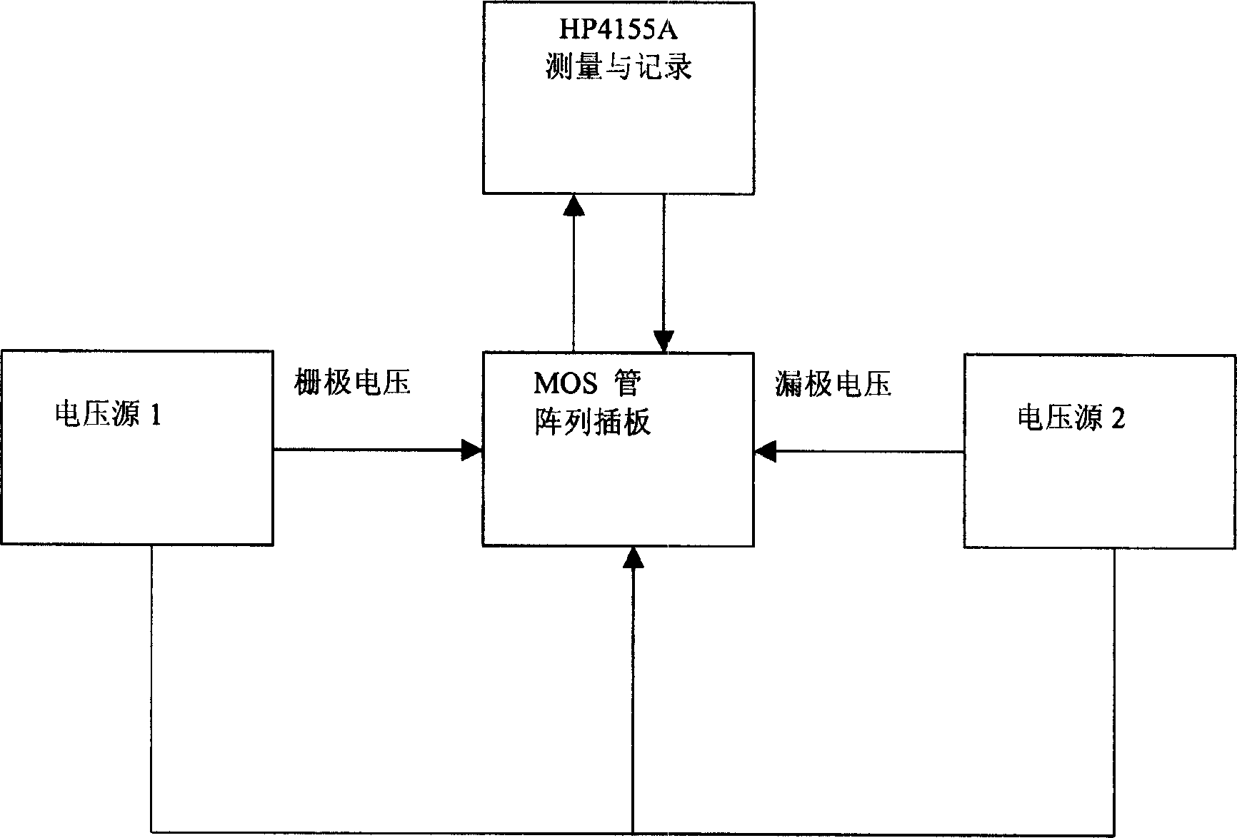
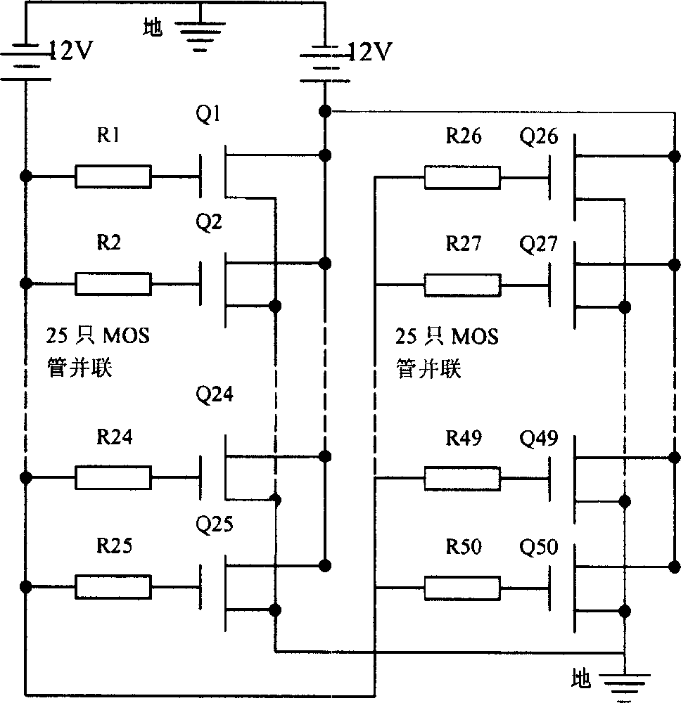
[0036] See Figure 1 to Figure 2As shown, the measurement method of the hot carrier injection effect of the MOS device of the present invention adopts HP4155A or the above series semiconductor parameter measuring instrument produced by Agilent Company (in this embodiment, the HP4155A semiconductor parameter measuring instrument is used for illustration), a self-made A measurement system composed of a circuit board with multiple (50 in this embodiment) sockets and a two-channel auxiliary voltage source, coupled with a batch data measurement and recording program written in BASIC language, is carried out as follows :

[0037] Step A: Determine the stress voltage value of the drain and gate of the device under test with HP4155A according to the standard;

[0038] Step B: Press the DISPLAY key twice on the panel of the HP4155A to display the program running interface, press the GET key and type in the program name, call out the data recording program written in BASIC language on ...


PUM


Abstract

The invention is a measuring method for MOS device heat carrier injecting effect. At first, the stress voltage value of drain and grid electrode of the device needed to be measured are determined according to the standard measuring device, and records the initial data through the data recording program; then the device needed to be measured is placed into the socket of the circuit board, at the same time, supplies voltage to the drain and grid electrode; shuts off the stress voltage at time point after 10, 20. and 50 seconds, the MOS is pulled out form the circuit board, and the degeneration quantity of designated parameter measured by the device are recorded; after the first time of data recording, all the MOS tubes are inserted into the original socket of the circuit board, then carries on correspondent voltage stress to the next time point, then stops the stress, then pulls out the MOS tubes form the circuit board, records the measured degeneration data, repeats the above mentioned steps until the degeneration quantity accords to the demands.

Description

【Technical field】 [0001] The invention relates to a measurement method, in particular to a measurement method for measuring the hot carrier injection effect of MOS devices in submicron and deep submicron integrated circuits. 【Background technique】 [0002] The hot carrier injection effect is an important failure mechanism of MOSFETs in modern submicron and deep submicron integrated circuits. High-energy carriers, also known as hot carriers, are generated from the large channel electric field of the drain of the MOSFET. This channel electric field will accelerate the hot carriers, making their effective temperature higher than the temperature of the lattice. These hot carriers transfer energy to the lattice through phonon emission, which will cause energy bond breaking at the Si / SiO2 interface, and hot carriers will also be injected into SiO2 and trapped. Bond breaking and trapped carriers generate oxide charges and interface states, which affect the channel carrier mobility...

Claims


Application Information

Patent Timeline
Patent Type & Authority Applications(China)
IPC IPC(8): G01R31/26H01L21/66
Inventor 章晓文
Owner 信息产业部电子第五研究所
Why Eureka
Try Eureka