


Quick Research
Generate reliable direction feasibility study reports for your R&D in just a few steps.

Technical Q&A
Discover and master advanced knowledge NOW. Basics, ideas, possibilities, all at once.

Find Solutions
As an expert in R&D theories, this can generate solutions to your technical problems instantly.

Evaluate Feasibility
Analyze your overall solution with one click, know your potential R&D risks in advance.

Monitor Landscape
Get weekly tech updates, stay abreast of the latest tech innovations and key insights.
Semiconductor device having multiple silicide types and a method for its fabrication
A metal silicide, oxide semiconductor technology, used in semiconductor/solid-state device manufacturing, semiconductor devices, electrical components, etc., to achieve the effect of reliable contact conditions
- Summary
- Abstract
- Description
- Claims
- Application Information
AI Technical Summary
Problems solved by technology
Method used
Image

Examples
no. 1 example
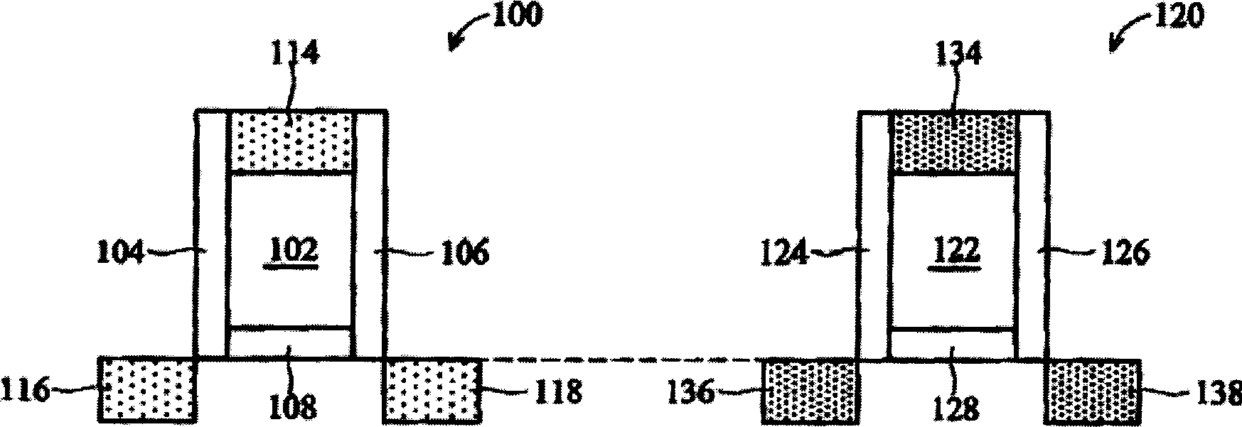
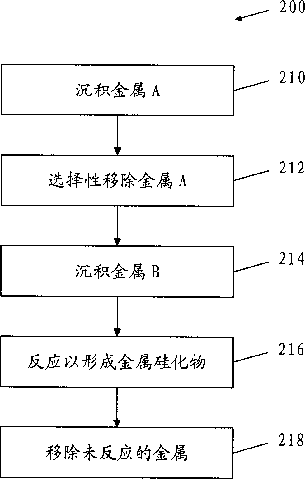
[0052] Such as Figure 2a , 2b to 2g. Figure 2a is a flowchart to illustrate the manufacturing figure 1 A first example method 200 is shown having a matched metal suicide structure of NMOS and PMOS. Figures 2b to 2g is adopted Figure 2a Shown is a first example method 200 of making figure 1 Schematic diagram of the process steps for the IC structure shown. It should be noted here that the method 200 is not limited to fabricating metal silicide structures matching NMOS and PMOS. In fact, it can be used to form any two metal silicide regions on a semiconductor substrate, wherein the first region has one composition or one material ratio, and the second region has a different composition or material ratio.
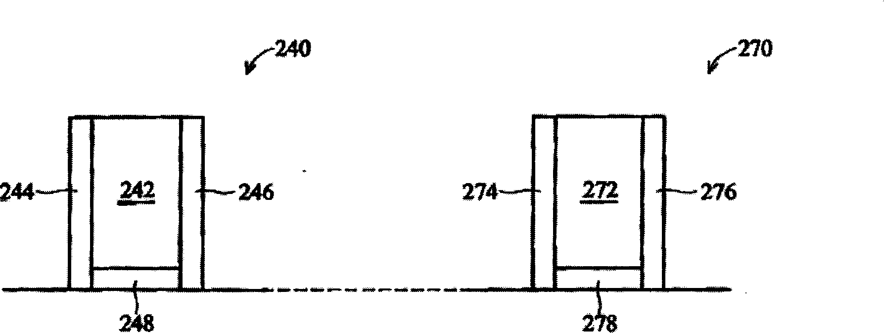
[0053] In this embodiment, the first area is NMOS240, and the second area is PMOS270, such as Figure 2b shown. It should be noted that before performing the method 200, the NMOS 240 and the PMOS 270 can be formed first. For example, the NMOS 240 includes a gate e...
PUM
| Property | Measurement | Unit |
|---|---|---|
| Work function | aaaaa | aaaaa |
| Work function | aaaaa | aaaaa |
Abstract
Description
Claims
Application Information
 - R&D Engineer
- R&D Manager
- IP Professional
- Industry Leading Data Capabilities
- Powerful AI technology
- Patent DNA Extraction
Browse by: Latest US Patents, China's latest patents, Technical Efficacy Thesaurus, Application Domain, Technology Topic, Popular Technical Reports.
© 2024 PatSnap. All rights reserved.Legal|Privacy policy|Modern Slavery Act Transparency Statement|Sitemap|About US| Contact US: help@patsnap.com