Separated grid flash memory unit and its mfg. method

A technology for separating gates and memory cells, which is applied in semiconductor/solid-state device manufacturing, electrical components, electric solid-state devices, etc. It can solve the problems of increasing component integration, increasing gate coupling rate, and failure to achieve, so as to increase the life of components , the effect of increasing reliability

Inactive Publication Date: 2005-03-09
POWERCHIP SEMICON CORP
View PDF0 Cites 6 Cited by
  • Summary
  • Abstract
  • Description
  • Claims
  • Application Information

AI Technical Summary

Problems solved by technology

However, in the existing split gate structure, the control gate and the floating gate form a stack structure, and the area between the control gate layer and the floating gate cannot be increased, resulting in the inability to increase the gate coupling. rate and the problem of increasing component integration

Method used


Image

  • Separated grid flash memory unit and its mfg. method
  • Separated grid flash memory unit and its mfg. method
  • Separated grid flash memory unit and its mfg. method

Examples


Embodiment Construction

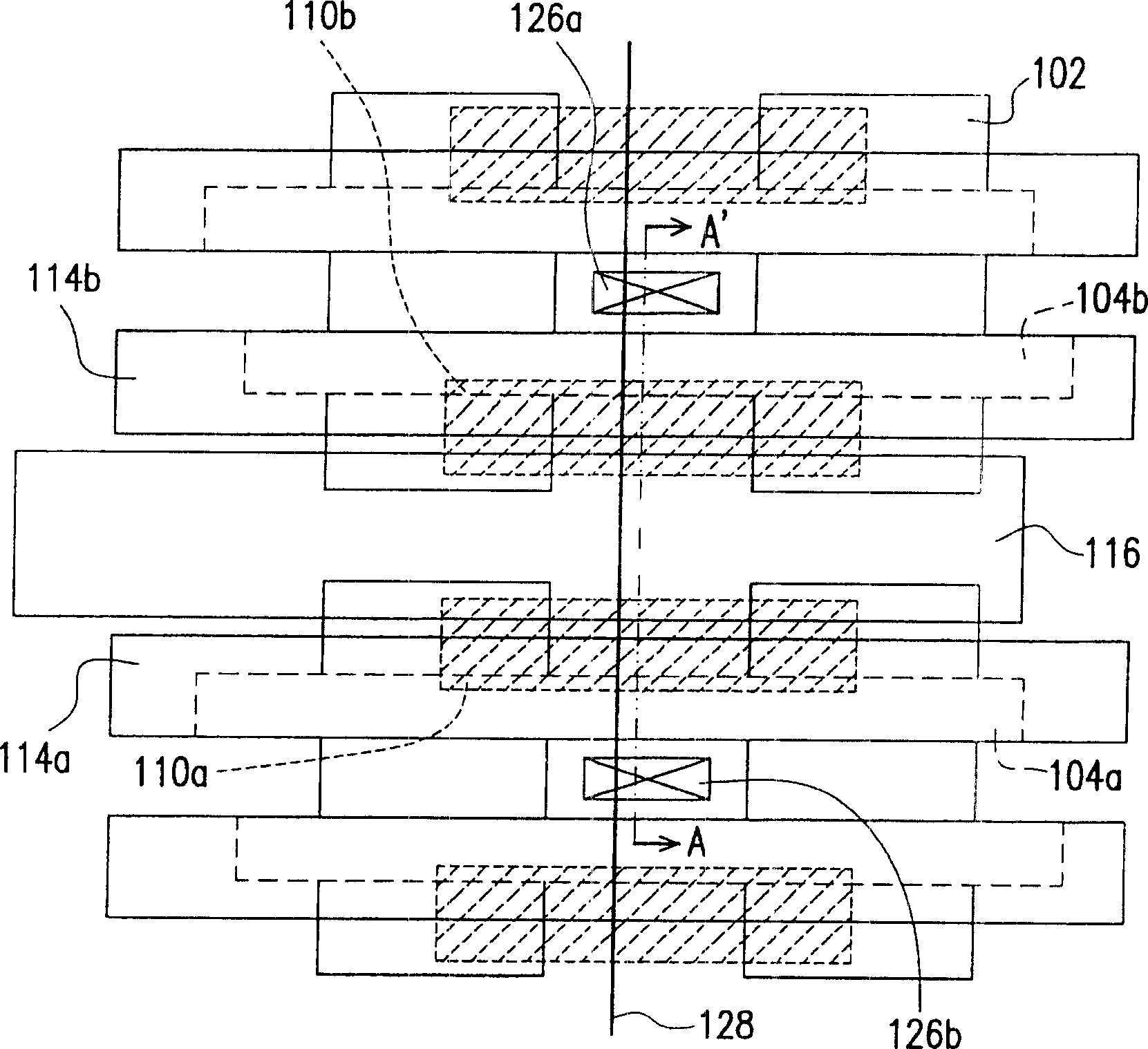
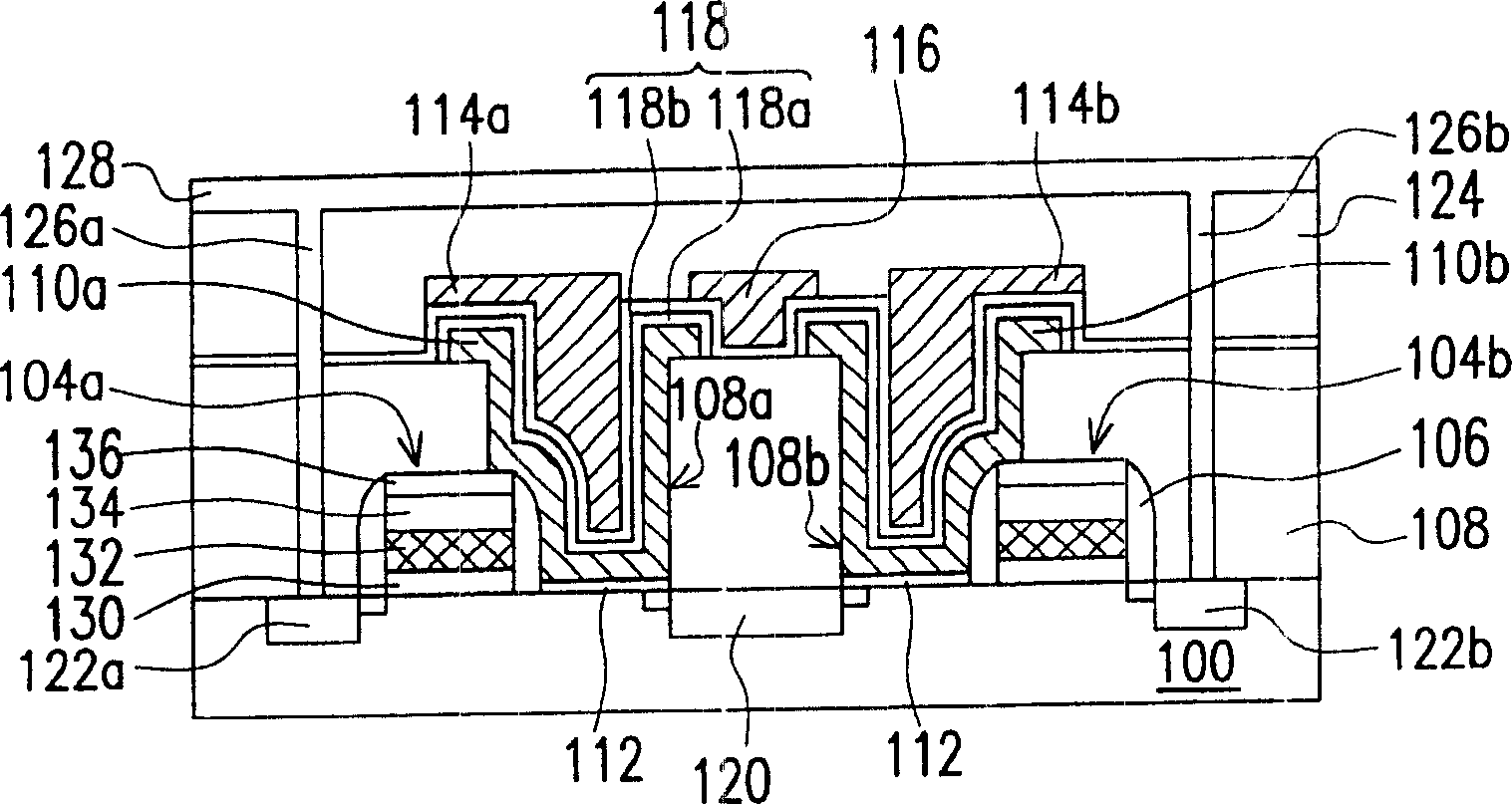
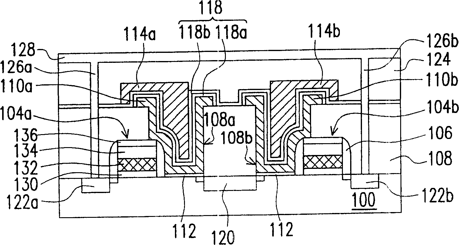
[0041] figure 1 Shown is a top view of a split gate flash memory cell according to an embodiment of the present invention. Figure 2A Shown is a cross-sectional view of the structure of the split-gate flash memory unit of the present invention. in, Figure 2A yes figure 1 The A-A line profile. Figure 2B Shown is a cross-sectional view of a split-gate flash memory cell according to another embodiment of the present invention. exist figure 1 , Figure 2A , Figure 2B In , the same components are given the same symbols, and descriptions thereof are omitted.

[0042] Please also refer to figure 1 and Figure 2A The flash memory unit of the present invention is composed of a substrate 100, an element isolation structure 102, a selection gate structure 104a and a selection gate structure 104b, a spacer 106, an interlayer dielectric layer 108, a floating gate 110a and a floating gate electrode 110b, tunneling dielectric layer 112, control gate 114a and control gate 114b, e...


PUM


Abstract

The present invention relates to a separate gate flash memory storage unit. It is includes substrate with element-isolating structure; selection gate structure placed on the substrate; interlaminar dielectric layer placed on the substrate and having opening, said opening expose partial selection gate structure, substrate and element-isolating structure; floating gate which is placed in the opening and whose part is extended to interlaminar dielectric layer surface; tunneling dielectric layer placed between floating gate and substrate; control gate which is placed in said opening, used for filling said opening and extented to the upper portion of selection gate structure; intergate dielectric layer placed between floating gate and control gate; source region placed in the substrate of one side of control gate which is not adjacent to selection gate structure and drain region placed in the substrate of one side of selection gate which is not adjacent to control gate.

Description

technical field [0001] The present invention relates to a semiconductor device, and in particular to a split gate flash memory unit and a manufacturing method thereof. Background technique [0002] Flash memory components have the advantages of being able to store, read, and erase data multiple times, and the stored data will not disappear after power failure, so it has become a widely used device for personal computers and electronic devices. A non-volatile memory element. [0003] A typical flash memory device uses doped polysilicon to make a floating gate (Floating Gate) and a control gate (Control Gate). Moreover, the floating gate is separated from the control gate by a dielectric layer, and the floating gate is separated from the substrate by a tunnel oxide layer (Tunnel Oxide). When writing / erasing (Write / Erase) data on the flash memory, by applying a bias voltage to the control gate and source / drain regions, electrons are injected into the floating gate or electron...

Claims


Application Information

Patent Timeline
Patent Type & Authority Applications(China)
IPC IPC(8): H01L21/8239H01L27/105
Inventor 吴陞黄财煜
Owner POWERCHIP SEMICON CORP
Why Eureka
Try Eureka