Image sensing assembly and its method
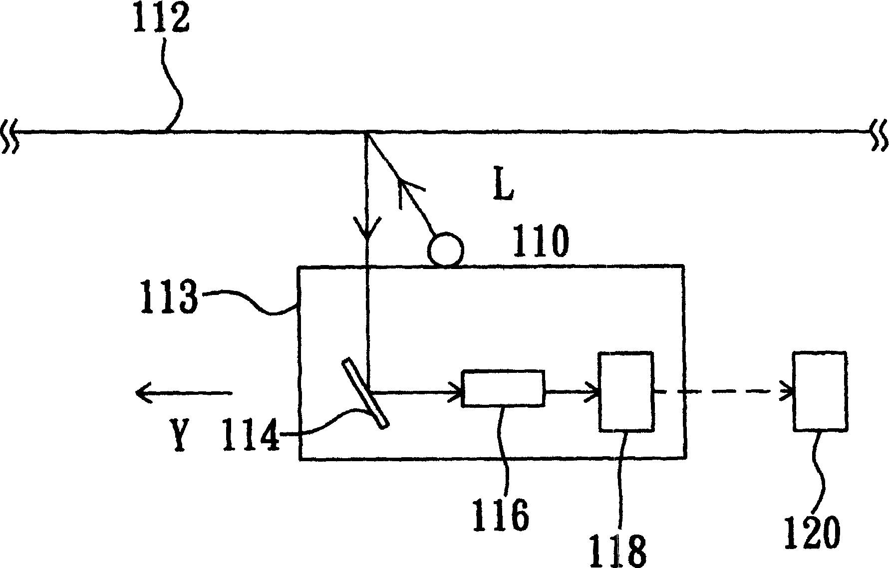
An image sensing and component technology, applied in image communication, electrical components, etc., can solve the problems of shortened lamp life, increased lamp 110, shortened exposure time of photosensitive components, etc.
- Summary
- Abstract
- Description
- Claims
- Application Information
AI Technical Summary
Problems solved by technology
Method used
Image
Examples
Embodiment Construction
[0022] specific implementation
[0023]The image sensing component of the present invention uses a CCD module used in a scanner as an example to illustrate how the image sensing component improves scanning resolution. As shown in FIG. 2(A), it is a schematic diagram of an image sensing component used in a scanner according to a preferred embodiment of the present invention. The scanner 200 includes an upper cover 210 and a base 220. The base 220 includes a scanning platform 221, an optical machine 223 and a circuit board 225. The scanning platform 221 is used to insert a document 222 to be scanned (taking a reflective document as an example), and the optical machine 223 also It includes a light source 224 , a mirror 226 , a lens group 227 and a CCD module 228 . When scanning documents, the light source 224 on the optical machine 223 projects a light L to the document 222 to be scanned. After being reflected by the document 222 to be scanned, the l...
PUM
 Abstract
Description
Claims
Application Information


