Methods of forming non-volatile resistance variable devices and methods of forming silver selenide comprising structures

A resistance device, silver selenide technology, applied in the direction of electric solid devices, electrical components, semiconductor devices, etc., can solve problems such as difficulty in forming silver selenide

Inactive Publication Date: 2005-07-27
MICRON TECH INC
View PDF4 Cites 2 Cited by
  • Summary
  • Abstract
  • Description
  • Claims
  • Application Information

AI Technical Summary

Problems solved by technology

However, it is difficult to form silver-rich silver selenide

Method used


Image

  • Methods of forming non-volatile resistance variable devices and methods of forming silver selenide comprising structures
  • Methods of forming non-volatile resistance variable devices and methods of forming silver selenide comprising structures
  • Methods of forming non-volatile resistance variable devices and methods of forming silver selenide comprising structures

Examples


Embodiment Construction

[0025] Detailed description of the preferred embodiment

[0026] The present disclosure is filed to further the fundamental purpose of the United States patent law, which is "to further the advancement of science and art" (Title 1, paragraph 8).

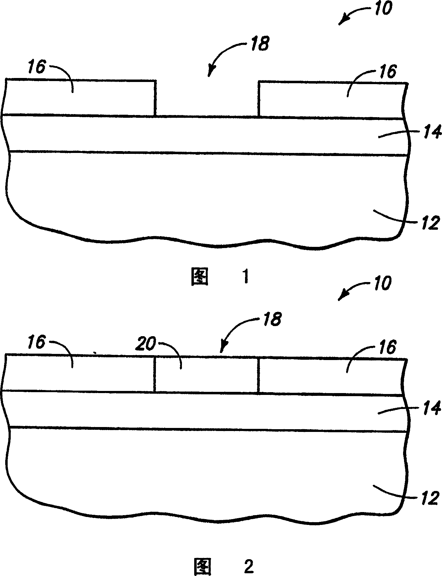
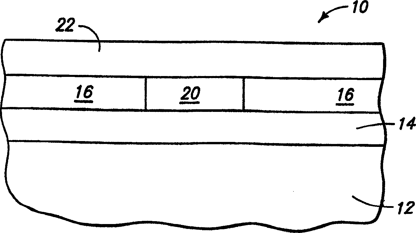
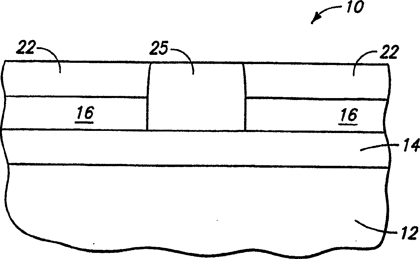
[0027] First refer to Figure 1 to Figure 8 Exemplary embodiments for forming non-volatile variable resistance devices are described. FIG. 1 depicts a substrate fragment 10 comprising a base substrate 12 and a first conductive electrode material 14 formed thereon. Base substrate 12 may include any suitable support substrate, for example, a semiconductor substrate including bulk monocrystalline Silicon. In the context of this document, the terms "semiconductor substrate" or "semiconducting substrate" are defined to mean any construction comprising semiconducting material, including but not limited to bulk semiconducting material such as a semiconducting wafer (either independently or in In a component on which other materials are c...


PUM


Abstract

A method of forming a non-volatile resistance variable device includes forming a patterned mass comprising elemental silver over a substrate. A layer comprising elemental selenium is formed over the substrate and including the patterned mass comprising elemental silver. The substrate is exposed to conditions effective to react only some of the elemental selenium with the elemental silver to form the patterned mass to comprise silver selenide. Unreacted elemental selenium is removed from the substrate. A first conductive electrode is provided in electrical connection with one portion of the patterned mass comprising silver selenide. A germanium selenide comprising material is provided in electrical connection with another portion of the patterned mass comprising silver selenide. A second conductive electrode is provided in electrical connection with the germanium selenide comprising material.

Description

technical field [0001] The present invention relates to methods of forming nonvolatile variable resistance devices and methods of forming structures comprising silver selenide. Background technique [0002] Semiconductor manufacturing continues efforts to make individual electronic devices smaller and smaller, resulting in denser integrated circuits. One class of integrated circuits includes memory circuits in which information is stored in the form of binary data. Circuitry can be fabricated such that data is either volatile or non-volatile. Volatile memory causes data loss when power is interrupted. Non-volatile memory circuits retain stored data even when power is interrupted. [0003] The present invention is primarily an improvement over the design and operation of memory circuits disclosed in U.S. Patent Nos. 5,761,115, 5,896,312, 5,914,893, and 6,084,796 to Kozicki et al., ultimately derived from U.S. Patent Application Serial No. filed on May 30, 1996 08 / 652,706 ...

Claims


Application Information

Patent Timeline
Patent Type & Authority Applications(China)
IPC IPC(8): H01L27/10H01L45/00
CPCH01L45/143H01L45/1675H01L45/085H01L45/1641H01L45/1683H01L45/1233H10N70/245H10N70/8825H10N70/826H10N70/041H10N70/066H10N70/063H01L27/10
Inventor T·L·吉尔顿K·A·坎贝尔J·T·穆尔
Owner MICRON TECH INC
Why Eureka
Try Eureka