
Exposure method, exposure apparatus, and method for manufacturing device

A technology of an exposure device and an exposure method, applied in the field of device manufacturing, can solve the problems of optical path length change, gas state destruction of projection optical system, gas leakage and the like

Inactive Publication Date: 2005-08-03
NIKON CORP
View PDF3 Cites 3 Cited by
  • Summary
  • Abstract
  • Description
  • Claims
  • Application Information

AI Technical Summary

Problems solved by technology

However, if the permeable gas flows into the optical path of the interferometer, the optical path length of the laser light will change due to the difference in the refractive index between the gas (air) and the permeable gas that existed on the interferometer optical path before then. Potentially reduce the control accuracy of the interferometer system
[0009] When the substrate is placed on the exit end side of the projection optical system, the substrate will become a part of the partition, so the leakage of the above-mentioned gas can be suppressed, but when moving the substrate or exchanging the substrate, at least part of the substrate that becomes the partition Part of it will leave the exit end side of the projection optical system, so that the state of the gas on the exit end side of the projection optical system will be destroyed, and the above-mentioned gas leakage will easily occur.

Method used


Image

  • Exposure method, exposure apparatus, and method for manufacturing device
  • Exposure method, exposure apparatus, and method for manufacturing device
  • Exposure method, exposure apparatus, and method for manufacturing device

Examples


Embodiment Construction

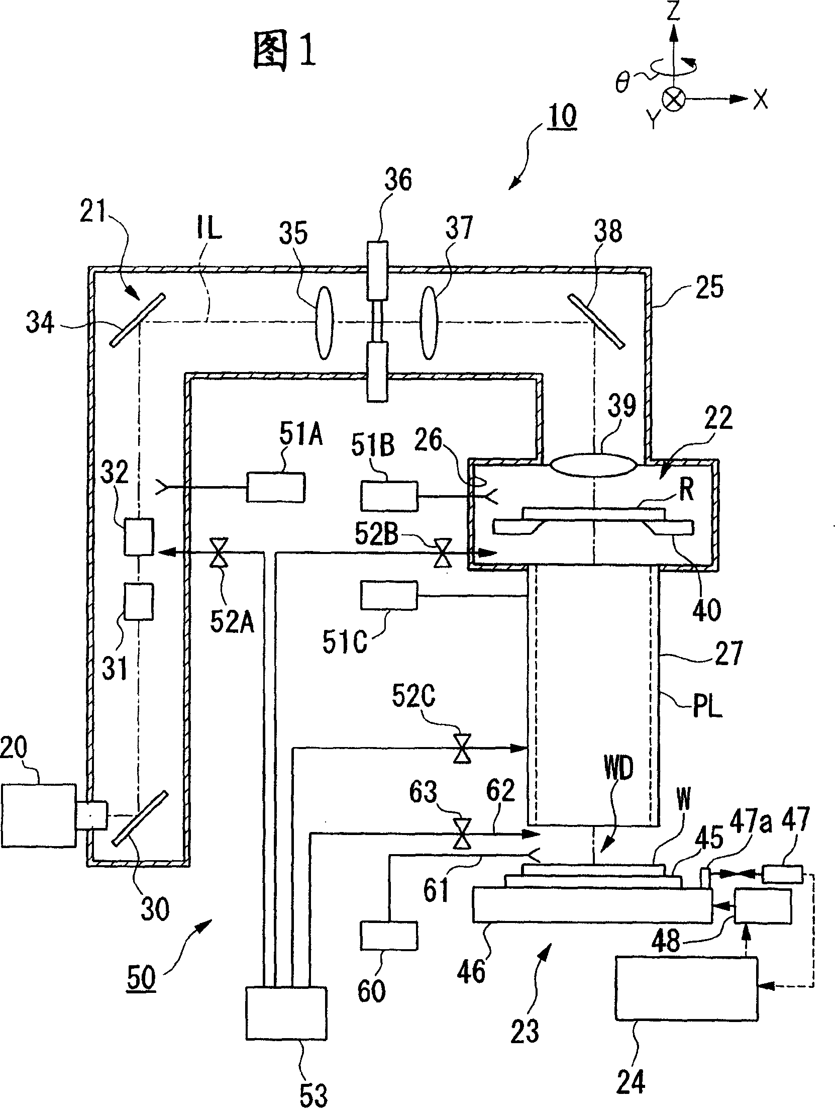
[0046] Embodiment 1 of the exposure apparatus of the present invention will be described below with reference to the drawings. In this embodiment, the present invention is applied to a step-and-scan projection exposure apparatus using vacuum ultraviolet light as an energy beam for exposure. However, the present invention is not limited to each of the following examples, and for example, these constituent elements may be appropriately combined.

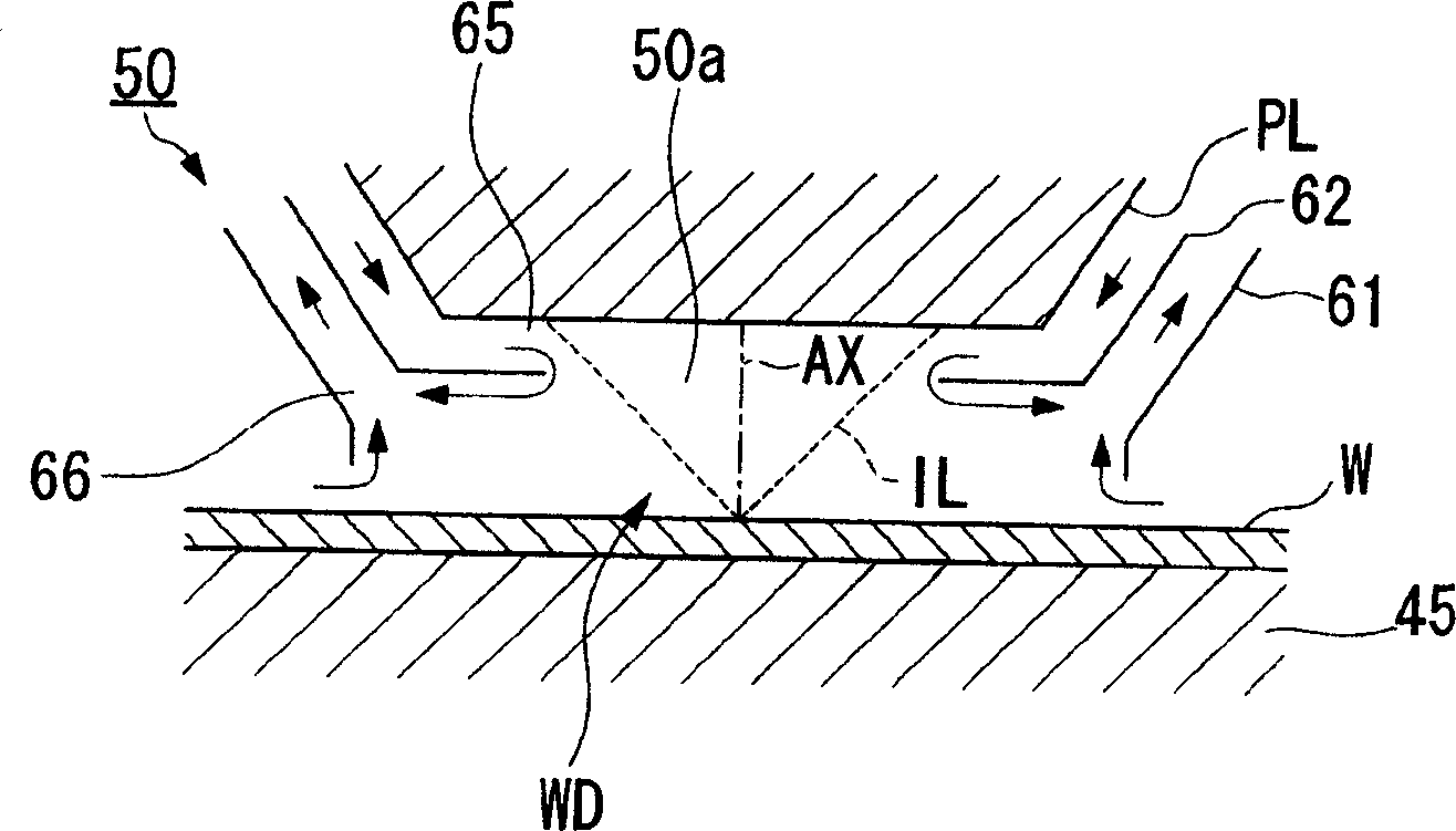
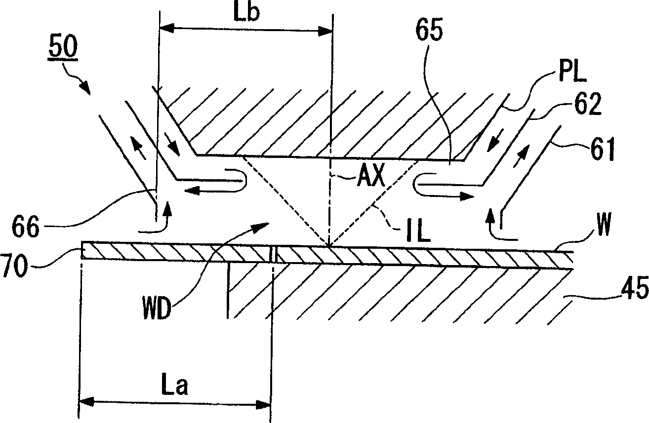
[0047] FIG. 1 is a partially cut-away configuration diagram showing a schematic configuration of an exposure apparatus 10 according to this embodiment. In FIG. 1 , the components of the exposure apparatus of this embodiment are mainly divided into an illumination optical system 21 , a reticle handling unit 22 , a projection optical system PL, and a wafer handling unit 23 . The illumination optical system 21, the reticle operating part 22, and the projection optical system PL are housed in a box-shaped illumination system chamber 25, r...


PUM

PropertyMeasurementUnit
wavelengthaaaaaaaaaa

Abstract

A substrate (W) serves as a part of a partition wall and an injection end side of a shot optical system (PL) is filled with a penetrating gas penetrating an energy beam (IL). When the substrate (W) is moved or exchanged, in order to maintain the gas state at the injection end side of the shot optical system (PL), an object (70) is arranged at the injection end side of the shot optical system (PL) instead of the substrate (W). Thus, it is possible to properly exclude light absorbing substance from the injection end side of the shot optical system and maintain the gas state even when the substrate is moved or exchanged.

Description

technical field [0001] The present invention relates to an exposure method and an exposure apparatus for manufacturing electronic devices such as semiconductor elements, liquid crystal display elements, imaging elements (CCD, etc.), and thin-film magnetic heads, and a method for manufacturing the devices. Background technique [0002] When electronic devices such as semiconductor elements and liquid crystal display elements are manufactured by photolithography, the image of the patterned mask or reticle (reticle - hereinafter referred to as reticle) is projected onto the photosensitive coating through the projection optical system. A projection exposure device for each projected (photographed) area on the substrate of the material (resist). The circuit of the electronic device is formed by exposing and transferring the circuit pattern on the exposed substrate by the above-mentioned projection exposure apparatus, and post-processing. [0003] In recent years, high-density in...

Claims


Application Information

Patent Timeline
Patent Type & Authority Applications(China)
IPC IPC(8): G03B27/52G03F7/20
CPCG03F7/70933G03F7/707G03F7/70733G03F7/70775G03F7/70808G03F7/70866G03F7/70908G03F7/20
Inventor 长坂博之青木贵史
Owner NIKON CORP
Learn More