

Display apparatus and driver circuit of display apparatus
A driver circuit, display device technology, applied in the direction of circuits, circuit devices, static indicators, etc.
- Summary
- Abstract
- Description
- Claims
- Application Information
AI Technical Summary
Problems solved by technology
Method used
Image

Examples
Embodiment approach 1
[0071] Use Figure 1~ image 3 and Figure 14 ~ Figure 18 An embodiment of the present invention is described as follows.
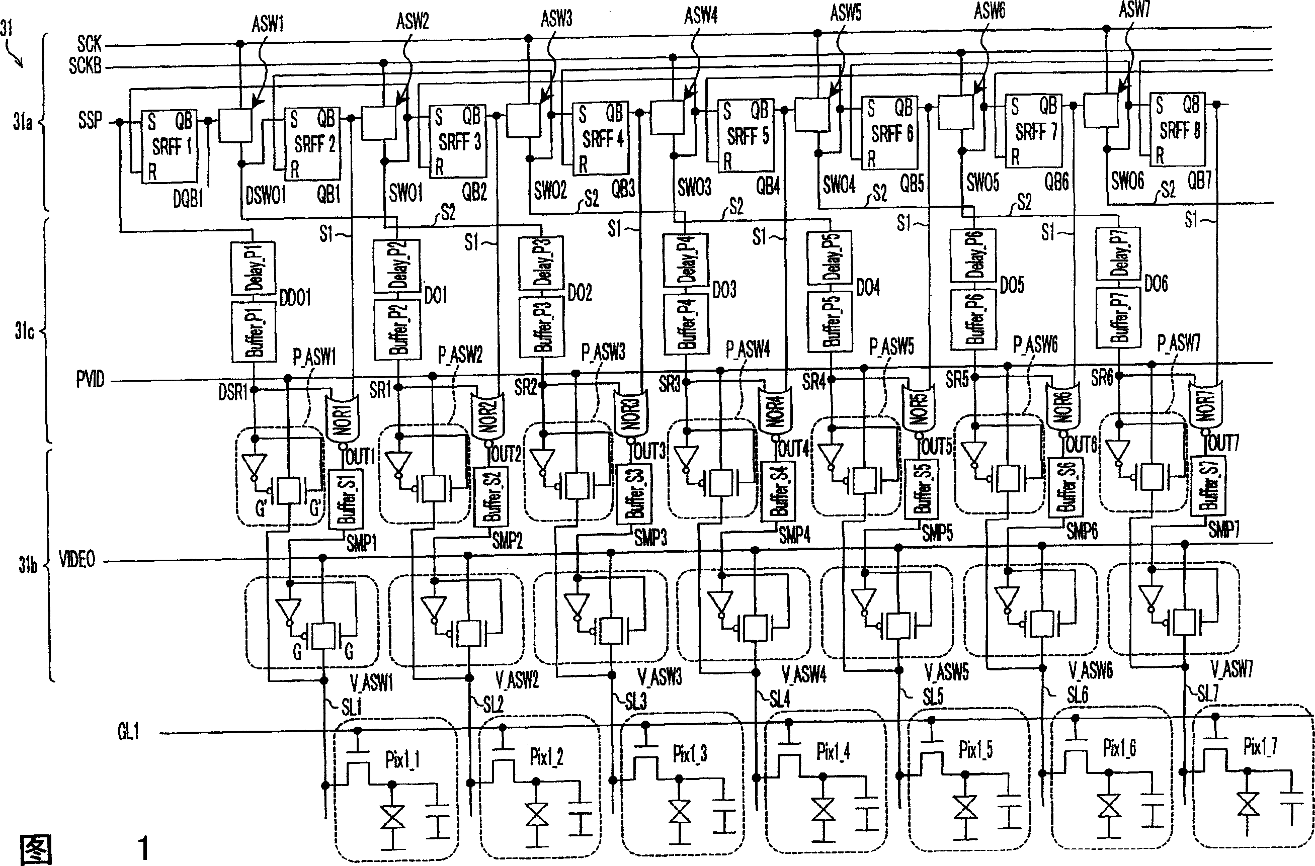
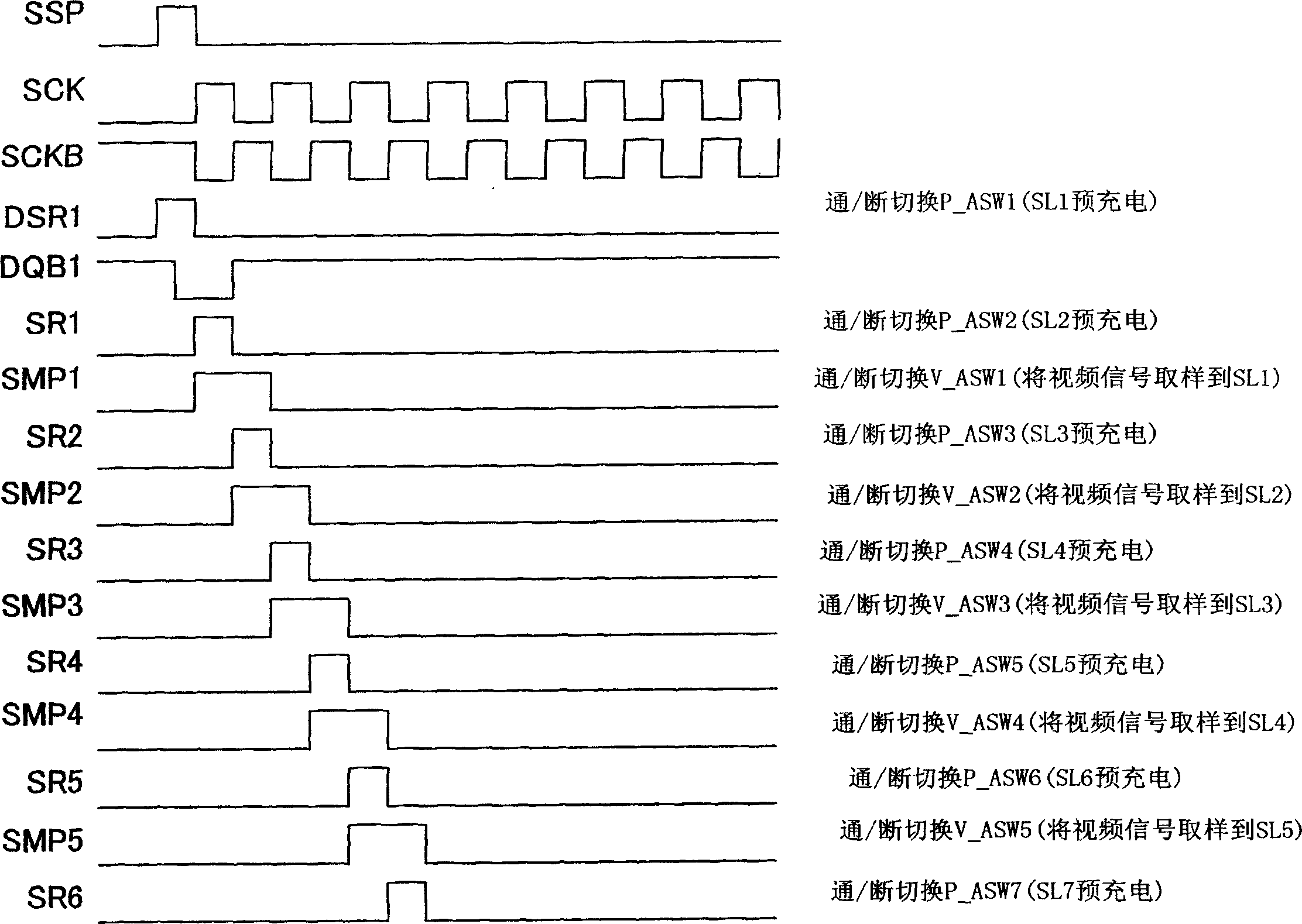
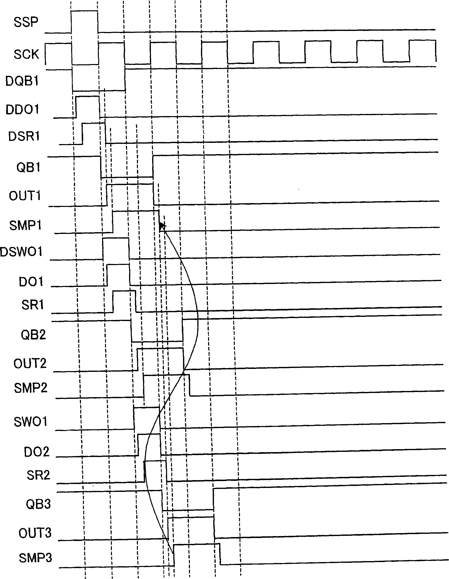
[0072] The display device driver circuit of this embodiment is a data signal line driver for a liquid crystal display device. FIG. 1 shows the composition of such a data signal line driver 31 .
[0073] The data signal line driver 31 has a shift register 31a, a sampling section 31b, and an overlap preventing section 31c.
[0074] The shift register 31a has multiple stages of set-reset flip-flops SRFF1, SRFF2, . . . , and a plurality of switch circuits (pulse signal supply circuits) ASW1, ASW2, . The switch circuit ASW k (k=1, 2, . . . ) uses the Q output of the flip-flop SRFF k as the control signal of conduction (on) and non-conduction (off). When the switch circuit ASW where k is an odd number is turned on, a clock signal (pulse signal, pulse for precharging) SCK supplied from an external supply source separate from the timing pulse described later i...
Embodiment approach 2
[0117] Using Figure 4 and Figure 5 Another embodiment of the present invention will be described as follows. For convenience of description, constituent units having the same functions as those described in Embodiment 1 are assigned the same reference numerals, their descriptions are omitted, and only differences will be described.
[0118] The display device driver circuit of this embodiment is a data signal line driver for a liquid crystal display device. FIG. 4 shows the composition of such a data signal line driver 32 .
[0119] The data signal line driver 32 has a shift register 32a, a sampling section 32b, and an overlap prevention section 32c.
[0120] The shift register 32a and the anti-overlapping unit 32c have the same composition as the shift register 31a and the anti-overlapping unit 31c in FIG. 1 , and only the composition of the sampling unit 32b is different. Specifically, the sampling unit 31b in FIG. 1 sets a dummy data signal line DSL connected to a dummy...
Embodiment approach 3
[0129] With Figure 7, Figure 8 and Figure 19 ~ Figure 2 1 Description Another embodiment of the present invention is as follows. Components having the same functions as those described in Embodiments 1 and 2 are denoted by the same reference numerals, and description thereof will be omitted.
[0130] The display device driver circuit of this embodiment is a data signal line driver for a liquid crystal display device. FIG. 7 shows the composition of such a data signal line driver 33. As shown in FIG.
[0131] The data signal line driver 33 has a shift register 33a, a sampling section 33b, and an overlap preventing section 33c.
[0132] The sampling unit 33b and the anti-overlapping unit 33c have the same composition as the sampling unit 31b and the anti-overlapping unit 31c in FIG. 1 , and only the composition of the shift register 33a is different.
[0133] The shift register 33a has flip-flops SRFF k (k=1, 2, . . . ) of FIG. 1 and level shifter circuits LSD0, LSD1, LS1,...
PUM
 Abstract
Description
Claims
Application Information