

Light-emitting device and display device
A technology for light-emitting devices and display devices, applied in lighting devices, luminescent materials, electroluminescent light sources, etc., can solve problems such as electrode damage, achieve stable productivity, reduce production costs, and suppress dielectric breakdown
- Summary
- Abstract
- Description
- Claims
- Application Information
AI Technical Summary
Problems solved by technology
Method used
Image

Examples
no. 1 approach
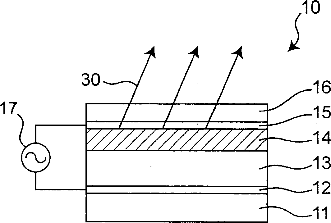
[0026] figure 1 It is a cross-sectional view perpendicular to the light emitting surface of the electroluminescence (EL) device 10 according to the first embodiment of the present invention. The EL device 10 is laminated on the back substrate 11 in sequence: the back electrode 12, the insulating layer 13 made of a dielectric material with a dielectric constant of 300 or more, and the inorganic phosphor powder dispersed in an organic binder The dispersed phosphor layer 14, the transparent front electrode 15, and the cover layer 16. The AC power source 17 arranged between the front electrode 15 and the back electrode 12 supplies an alternating voltage to cause the dispersion type phosphor layer 14 to emit. The light 30 emitted from the phosphor layer 14 emits light in all directions, and is obtained through the transparent front electrode side in the EL device 10. Because the insulating layer 13 is an annealed dielectric material, the surface roughness of the insulating layer 13 i...
no. 2 approach
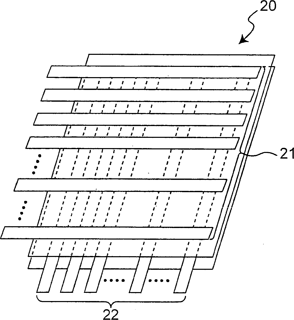
[0051] Below, reference figure 2 The display device according to the second embodiment of the present invention is described. figure 2 Shown is a schematic plan view of a passive matrix display device 20 having a transparent electrode 21 and a counter electrode 22 perpendicular to each other. This display device 20 has a plurality of EL devices as described in the above-mentioned first embodiment arranged in a plane. The plurality of transparent electrodes 21 are parallel to the first direction and parallel to the surface of the EL array, and the plurality of opposite electrodes 22 are parallel to the surface of the EL array and parallel to the second direction perpendicular to the first direction. In this display device 20, the reverse electrode 22 is connected to the back electrode of each EL device, and the transparent electrode 21 is connected to the front electrode of each EL device. An external AC voltage is applied between the pair of transparent electrodes 21 and the cou...
Embodiment 1
[0056] The EL device according to this embodiment is basically the same as the above-mentioned basis figure 1 The EL device of the first embodiment shown is the same, except that it has no cover layer. The method of preparing this EL device is described below:
[0057](a) A 0.635 mm thick alumina substrate is used for the back substrate.
[0058] (b) An Ag-Pd paste of about 85% Ag and about 15% Pd was used for the back electrode, and a stripe pattern of 2 mm wide lines with a pitch of 3 mm was screen printed on the back substrate. The paste is then dried and annealed to obtain an Ag-Pd alloy back electrode on the back substrate.
[0059] (c) BaTiO 3 The paste is used as a precursor of the dielectric material of the insulating layer, and this paste is screen printed on the back electrode. Then the paste was annealed at 950°C in an air atmosphere to form BaTiO on the back electrode 3 Insulation. The film thickness of the resulting insulating layer was 35 μm, and the center line ave...
PUM
| Property | Measurement | Unit |
|---|---|---|
| thickness | aaaaa | aaaaa |
| height | aaaaa | aaaaa |
| thickness | aaaaa | aaaaa |
Abstract
Description
Claims
Application Information