Optical signal receiver, optical signal receiving apparatus, and optical signal transmitting system

一种传送系统、接收装置的技术,应用在传输系统、电磁波传输系统、光纤传输等方向,能够解决相位失真、延迟线不同延迟时间特性、阻抗不匹配等问题,达到高频相位失真改善、良好传送特性的效果

Inactive Publication Date: 2005-12-07
NIPPON TELEGRAPH & TELEPHONE CORP
View PDF3 Cites 8 Cited by
  • Summary
  • Abstract
  • Description
  • Claims
  • Application Information

AI Technical Summary

Problems solved by technology

[0045] However, in the existing FM demodulation circuit, the delay line has different delay time characteristics in low frequency and high frequency due to impedance mismatch at both ends of the delay line 132 used in delay line detection, etc.
[0046] That is, phase distortion occurs in low and high frequencies
As a result, CSO, CTB will be degraded due to phase distortion of low frequency and high frequency

Method used


Image

  • Optical signal receiver, optical signal receiving apparatus, and optical signal transmitting system
  • Optical signal receiver, optical signal receiving apparatus, and optical signal transmitting system
  • Optical signal receiver, optical signal receiving apparatus, and optical signal transmitting system

Examples


Embodiment approach 1

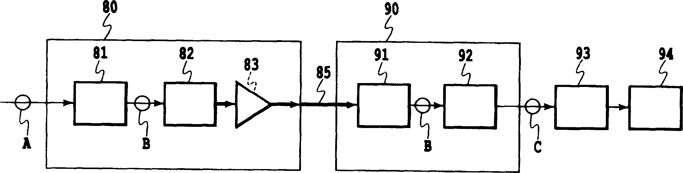
[0086] This embodiment is an optical signal receiver that performs delay detection using an optical delay line. Figure 10 The structure of the optical signal receiver according to this embodiment is shown in . Figure 10 The optical signal receiver 10 shown in the figure has an optical amplifier circuit 11, an optical branch circuit 13, an optical delay line 15, a first photoelectric conversion circuit 17, a first identification circuit 21, a second photoelectric conversion circuit 19, and a second identification circuit 23. Logic AND circuit 25, and smoothing circuit 12.

[0087] refer to Figure 10 The structure of the optical signal receiver of this embodiment will be described. Figure 10 The optical signal receiver 10 shown in has the function of receiving and demodulating the frequency modulated optical signal. Each circuit of the optical signal receiver and its operation will be described. The optical amplifier circuit 11 optically amplifies the input optical signa...

Embodiment approach 2

[0101] This embodiment is an optical signal receiver that performs delay detection using an optical delay line. Figure 13 The structure of the optical signal receiver according to this embodiment is shown in . Figure 13 The optical signal receiver 10 shown in the figure has an optical amplifier circuit 11, an optical branch circuit 13, an optical delay line 15, a first photoelectric conversion circuit 17, a first identification circuit 21, a second photoelectric conversion circuit 19, and a second identification circuit 23. Logic OR circuit 27, and smoothing circuit 12.

[0102] refer to Figure 13 The structure of the optical signal receiver of this embodiment will be described. Figure 13The optical signal receiver 10 shown in has the function of receiving and demodulating the frequency modulated optical signal. Each circuit of the optical signal receiver and its operation will be described. The optical amplifier circuit 11 optically amplifies an input optical signal. ...

Embodiment approach 3

[0116] This embodiment is an optical signal receiver that performs delay detection using an optical delay line. Figure 16 The structure of the optical signal receiver according to this embodiment is shown in . Figure 16 The optical signal receiver 10 shown in has an optical amplifier circuit 11, an optical branch circuit 13, an optical delay line 15, a first photoelectric conversion circuit 17, a first limiting amplifier circuit 41, a second photoelectric conversion circuit 19, a second Limiting amplifier circuit 42 , adding circuit 43 , high level discriminator 44 , and smoothing circuit 12 .

[0117] refer to Figure 16 The structure of the optical signal receiver of this embodiment will be described. Figure 16 The optical signal receiver 10 shown in has the function of receiving and demodulating the frequency modulated optical signal. Each circuit of the optical signal receiver and its operation will be described. The optical amplifier circuit 11 optically amplifies ...


PUM


Abstract

The optical signal receiver of this invention is an optical signal receiver that receives and frequency-demodulates an optical signal, comprising: an optical branch device for splitting an input optical signal into two optical signals ( 13 ); an optical delay line for delaying one of the two branched optical signals ( 15 ); a first photoelectric conversion circuit ( 17 ) for converting the optical signal from the optical delay line into the first electrical signal ( 17 ); a second photoelectric conversion circuit ( 19 ) for converting the other optical signal of the two branched optical signals into a second electrical signal; the rectangular-wave forming circuit ( 21, 23, 25 ) for outputting a single rectangular-wave signal using the first electrical signal from the first photoelectric conversion circuit and the second electrical signal from the second photoelectric conversion circuit as inputs; and a smoothing circuit ( 12 ) for smoothing the rectangular-wave signal from the rectangular-wave forming circuit.

Description

technical field [0001] The present invention relates to an optical signal receiver for transmitting an optical signal subjected to frequency modulation (FM: Frequency Modulation) of a broadband signal, an optical signal receiving device, and an optical signal using the optical signal receiver or the optical signal receiving device delivery system. In more detail, it relates to an optical signal receiver for transmitting an optical signal of a frequency division multiplexed multi-channel image signal subjected to amplitude modulation (AM: Amplitude Modulation) or quadrature amplitude modulation (QAM: Quadrature Amplitude Modulation), An optical signal receiving device and an optical signal transmission system using the optical signal receiver or the optical signal receiving device. Background technique [0002] At present, as an optical signal receiver, an optical signal receiving device, and an optical signal transmission system for optically transmitting an amplitude-modul...

Claims


Application Information

Patent Timeline
Patent Type & Authority Applications(China)
IPC IPC(8): H04B10/516H04B10/2507H04B10/54H04B10/548H04B10/58H04B10/61
CPCH04B10/66
Inventor 菊岛浩二
Owner NIPPON TELEGRAPH & TELEPHONE CORP
Why Eureka
Try Eureka