Spring surface acoustic wave device manufacturing method, spring surface acoustic wave device

A technology of surface acoustic wave and a manufacturing method, which is applied in the manufacture of surface acoustic wave devices and the field of surface acoustic wave devices, can solve problems such as the insulation properties of harmful surface acoustic wave components, achieve good insulation properties, high-function communication devices, prevent thermoelectricity the effect of destruction

Active Publication Date: 2006-01-04
KYOCERA CORP
View PDF0 Cites 5 Cited by
  • Summary
  • Abstract
  • Description
  • Claims
  • Application Information

AI Technical Summary

Problems solved by technology

[0024] The inventors of the present invention have found that the above-mentioned inner conductor layer 59 can effectively prevent pyroelectric destruction in the device manufacturing process, but it is detrimental to the insulation properties of the surface acoustic wave device.

Method used


Image

  • Spring surface acoustic wave device manufacturing method, spring surface acoustic wave device
  • Spring surface acoustic wave device manufacturing method, spring surface acoustic wave device
  • Spring surface acoustic wave device manufacturing method, spring surface acoustic wave device

Examples


Embodiment 1

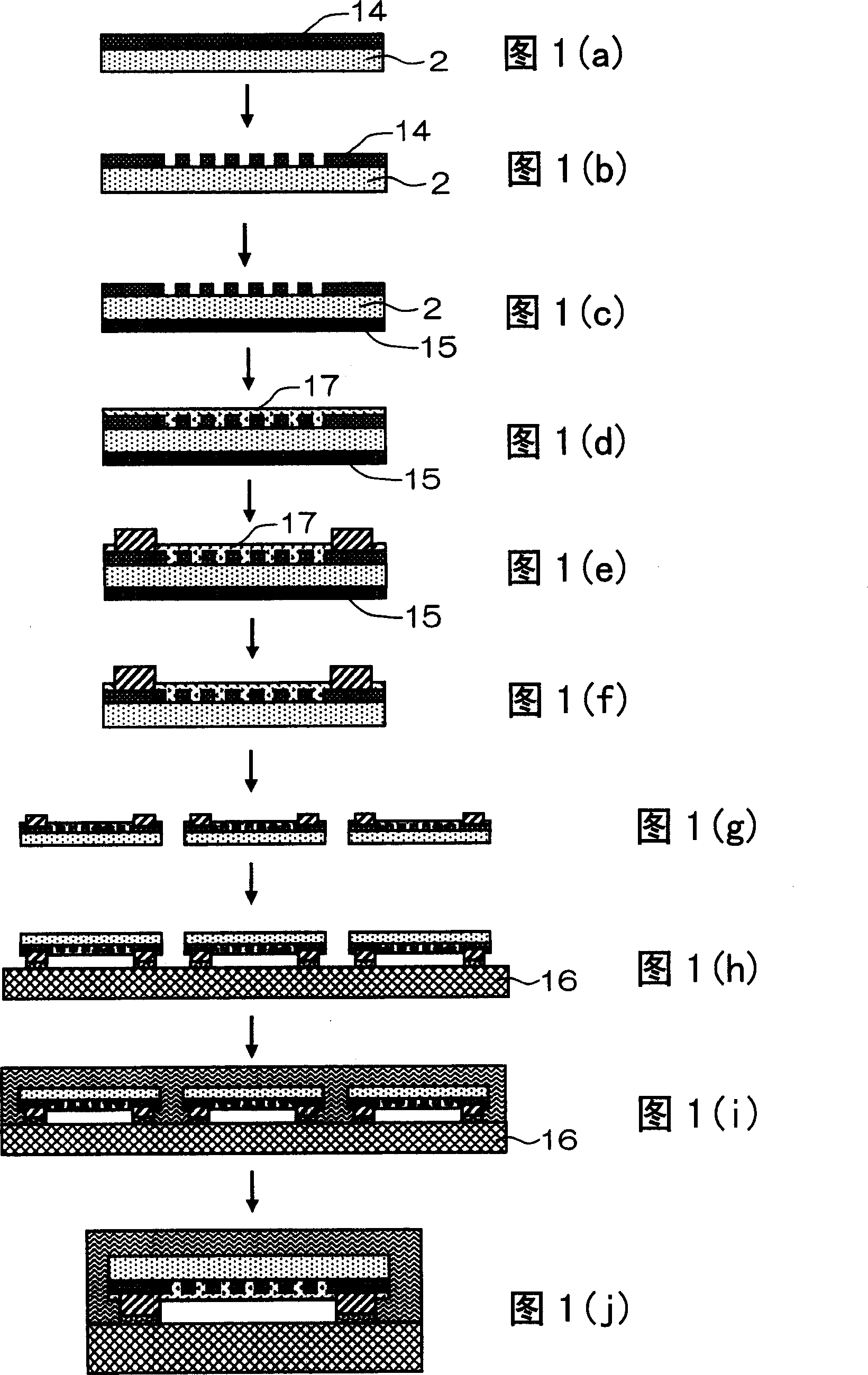
[0145] A surface acoustic wave device was manufactured by the method shown in FIG. 1( a ) to FIG. 1( j ).

[0146] The main surface of the piezoelectric substrate 2 (substrate thickness: 250 μm) formed on the lithium tantalate single crystal substrate in the Y-cut X-transport direction at 38.7° is formed into a film of Ti / Al-1 mass% Cu / Ti from the substrate side by sputtering 4-layer electrode layer formed of / Al-1 mass% Cu. The film thicknesses are 6nm / 209nm / 6nm / 209nm, respectively.

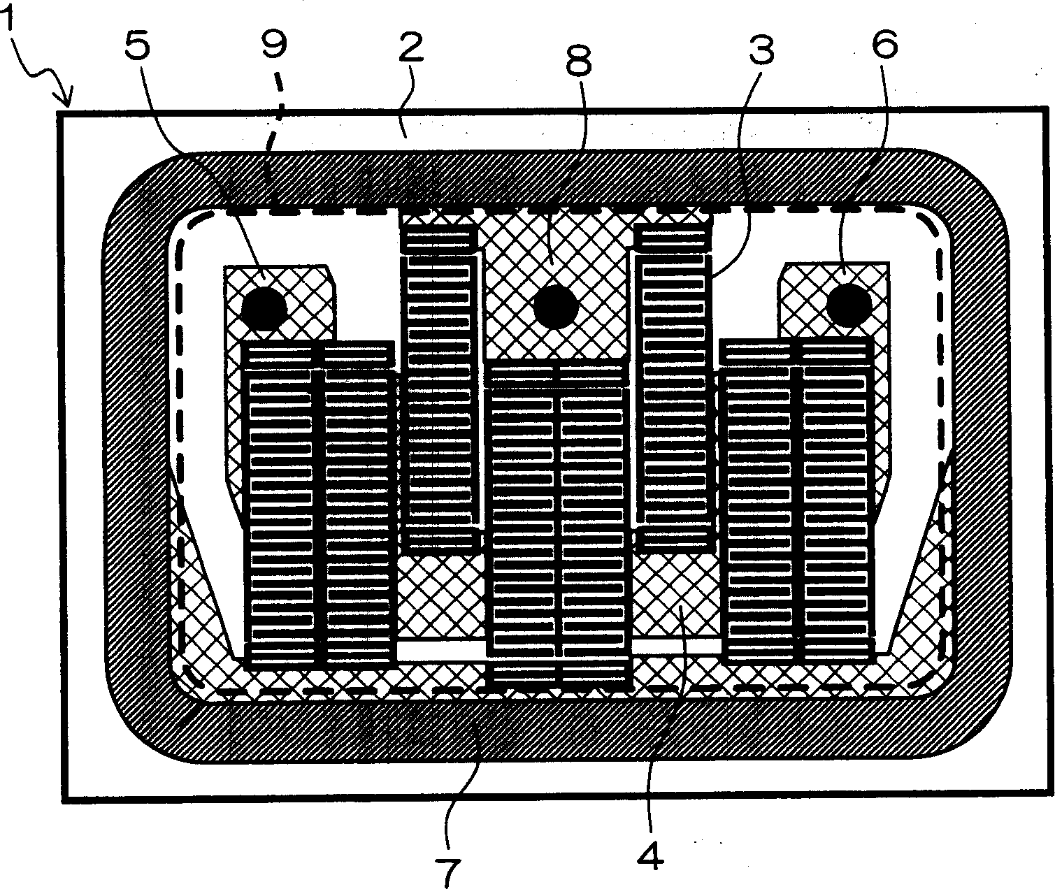
[0147] Next, if image 3 As shown, the electrode layer is patterned by photolithography and RIE to form a plurality of surface acoustic wave element regions, which have: filter regions having IDT electrodes 3 , input electrode parts 5 and output electrode parts 6 are formed. In addition, at this time, the ground electrode portion 8 , the connection electrode 4 and the annular electrode 7 are also formed simultaneously.

[0148] As the etching gas at this time, a mixed gas of BC13 and C12 was ...

Embodiment 2

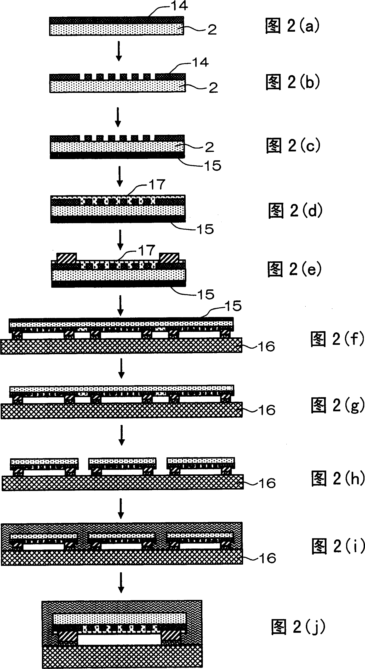
[0166] A duplexer-type surface acoustic wave device having a transmission-side filter region and a reception-side filter region in a piezoelectric substrate was fabricated by the method shown in FIGS. 1( a ) to 1( j ).

Embodiment 2-1

[0168] As in Example 1, four electrode layers were formed on the main surface of the lithium tantalate single crystal substrate.

[0169] Next, the electrode layer is patterned by photolithography and RIE to form a plurality of filter regions, which have the following functions: forming a transmission-side filter region with an IDT electrode 3, an input electrode portion 5, and an output electrode portion 6 and a reception-side filter region; device area. In addition, at this time, the ground electrode portion 11 , the connection electrode 4 , and the annular electrode 7 are also formed at the same time.

[0170] As the etching gas at this time, a mixed gas of BC13 and C12 was used.

[0171] The line width of the comb-shaped electrodes forming the IDT electrodes 3 and the distance between adjacent comb-shaped electrodes are both approximately 1 μm.

[0172] Next, a conductor layer made of pure Al was formed on the other surface of the piezoelectric substrate 2 by a sputterin...


PUM


Abstract

After an electrode figure (the figure 1 (b)) is formed in an electrode forming side of a piezoelectricity base plate (2), a conductor layer (the figure 1 (c)) is formed in a non-forming electrode side of the piezoelectricity base plate (2). After the conductor layer is formed, at least one working procedure (the figure 1 (e)) is processed, and the conductor layer which is formed at the other side is removed (as the figure 1 (f)), cutting for dividing each element is processed, and the base plate used for installing is installed. The conductor layer at the other side of the piezoelectricity base plate is removed entirely, which can improve attenuation outside strip region and insulating characteristic greatly.

Description

technical field [0001] The present invention relates to a method of manufacturing a surface acoustic wave device used in a surface acoustic wave (surface acoustic wave) filter, etc., a surface acoustic wave device, and a communication device. Background technique [0002] In recent years, surface acoustic wave filters have been applied to various communication devices. [0003] With the development of higher frequency and higher functionality of communication devices, there is an increasing need to increase the out-of-band attenuation (attenuation) of surface acoustic wave filters. [0004] Figure 13 A schematic cross-sectional view of a flip-chip structure of a conventional surface acoustic wave device is shown in . [0005] Figure 13 Among them, 51 is a piezoelectric substrate, 52 is a ground pad, 53 is a comb-shaped IDT (Inter Digital Transducer) electrode (referred to as an IDT electrode) formed on the piezoelectric substrate 51, and 54 is an electrode formed on the p...

Claims


Application Information

Patent Timeline
Patent Type & Authority Applications(China)
IPC IPC(8): H03H3/08H03H9/25
Inventor 横田裕子伊藤干饭冈淳弘古贺亘长峰成彦
Owner KYOCERA CORP
Why Eureka
Try Eureka