Supercharge Your Innovation With Domain-Expert AI Agents!

Alloy material for semiconductor, semiconductor chip using such alloy material, and method for manufacturing same

A technology of alloy materials and semiconductors, which is applied in semiconductor/solid-state device manufacturing, semiconductor devices, metal material coating processes, etc., can solve the problems of uneven alloy layer, reduced stability of alloy layer composition, and complicated methods.

Inactive Publication Date: 2006-01-04
SHARP KK +1
View PDF1 Cites 2 Cited by
  • Summary
  • Abstract
  • Description
  • Claims
  • Application Information

AI Technical Summary

Problems solved by technology

[0008] However, the alloy layer formed using these targets may be non-uniform, causing a problem that the compositional stability of the alloy layer decreases
In addition, a method involving diffusion after forming a multilayer film increases the number of manufacturing steps, making the method complicated
Furthermore, there are limitations to the homogeneity achievable by diffusion
Therefore, it is difficult to form a uniform alloy layer
[0009] In other words, under existing circumstances, single-layer films of Au / Ag alloys cannot be used in semiconductor applications as a material that compensates for the disadvantages of Au and Ag while maximizing the advantages of both.

Method used


Image

  • Alloy material for semiconductor, semiconductor chip using such alloy material, and method for manufacturing same
  • Alloy material for semiconductor, semiconductor chip using such alloy material, and method for manufacturing same
  • Alloy material for semiconductor, semiconductor chip using such alloy material, and method for manufacturing same

Examples


Embodiment 1

[0054] Embodiment 1: the preparation of alloy material

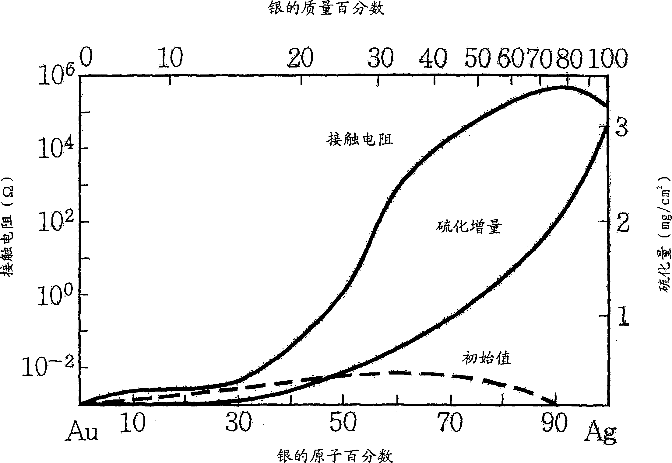
[0055] Au ingots and Ag ingots were weighed so that Au and Ag had different ratios, and after melting these ingots by high-frequency melting, Au and Ag were poured into a mold to prepare an AuAg alloy material. Au and Ag with a purity of 4N were used as raw materials.

[0056] The obtained alloy materials with different compositions were made into samples with respective dimensions of about 50×20×1, and the samples were kept at 60°C, 90mmHg, H 2 S atmosphere for 10 days. The samples were then measured separately to obtain the relationship between the composition of the sample and the amount of vulcanization, and the relationship between the composition of the sample and the contact resistance. The contact resistance before and after the vulcanization test was measured by a four-terminal method. The vulcanization increment was determined from the weight of the sample before and after the vulcanization test using a prec...

Embodiment 2

[0060] Embodiment 2: the preparation of alloy material

[0061] 7.5 kg of an Au ingot with a purity of 4N and 2.5 kg of an Ag ingot with a purity of 4N were put into a crucible and melted by a high-frequency melting method. Au and Ag are then poured into a mold to prepare an alloy ingot with an Au-Ag ratio of 75%-25%. The thus obtained AuAg alloy material has the machinability of Au and the ductility of Ag.

[0062] The resulting alloy ingots were rolled to form 8 mm thick plates. The plate was formed into a 250 mm diameter disk on a lathe and bonded to a backing plate made of Cu to prepare an AuAg alloy target. For comparison, Au targets and Ag targets were prepared in the same manner as AuAg alloy targets.

Embodiment 3

[0063] Embodiment 3: the preparation of alloy material

[0064] AuAg alloy targets were prepared in the same manner as in Example 2, except that the proportion of Ag was set to 3 wt%, 10 wt%, and 40 wt%.


PUM

PropertyMeasurementUnit
thicknessaaaaaaaaaa
diameteraaaaaaaaaa
thicknessaaaaaaaaaa

Abstract

An alloy material for semiconductors mainly contains Au and includes 3-40 wt% of Ag.

Description

technical field [0001] The invention relates to an alloy material for semiconductors, a semiconductor chip using the alloy material and a method for preparing the semiconductor chip. More particularly, the present invention relates to an AuAg alloy material, to a semiconductor chip using the alloy material for chip stability, and to a method of manufacturing the semiconductor chip. Background technique [0002] Conventionally, as materials for manufacturing semiconductor devices, Au and Ag have been used in the form of a single layer according to their usage purposes. [0003] Generally, Au is a metallic material that is stable in air and has good ductility. Even when heated, Au does not react with components or other materials in the atmosphere, and can maintain a clean metal surface. In addition, Ag is cheap and has low resistance. For the above reasons, Au is often used as a metal material for semiconductors. [0004] However, when the Au film is directly applied on t...

Claims


Application Information

Patent Timeline
Patent Type & Authority Applications(China)
IPC IPC(8): H01L21/28H01L21/285H01L21/288H01L21/3205C23C14/34C23C14/24C22C5/02
CPCC22C5/02H01L24/43H01L24/45H01L2224/45015H01L2224/45144H01L2224/48247H01L2924/01047H01L2924/01204H01L2924/20752H01L2924/20753H01L2924/013H01L2924/00H01L21/00
Inventor 井上和范石仓千春
Owner SHARP KK
Features
  • R&D
  • Intellectual Property
  • Life Sciences
  • Materials
  • Tech Scout
  • Unparalleled Data Quality
  • Higher Quality Content
  • 60% Fewer Hallucinations
Learn More