
Electro-optical device, method of manufacturing the same, and electronic apparatus using electro-optical device

An electro-optic device and manufacturing method technology, applied in optics, nonlinear optics, static indicators, etc., can solve problems such as defective products, difficulty in drawing spacers, and difficulty in homogenizing products

Inactive Publication Date: 2006-01-18
SEIKO EPSON CORP
View PDF1 Cites 10 Cited by
  • Summary
  • Abstract
  • Description
  • Claims
  • Application Information

AI Technical Summary

Problems solved by technology

[0015] However, if the distance between the opposing substrates is narrowed, it will be difficult to draw the spacer with a dispenser or the like on the boundary between the opposing substrates, and the spacer will only be drawn on the peripheral edge of the lens glass substrate.
As a result, as the distance between the lens glass substrate and the cover glass substrate transitions from the outer edge to the center, the amount of deflection gradually increases, and the thickness of the microlens layer tends to vary accordingly, maintaining the homogeneity of the product. become difficult
[0016] Although the deviation of the thickness of the microlens layer in a large substrate is within the error range, it does not directly lead to defective products, but with the recent demand for high image quality, higher precision is required for the thickness of the microlens layer , becomes an obstacle to satisfying the requirement

Method used


Image

  • Electro-optical device, method of manufacturing the same, and electronic apparatus using electro-optical device
  • Electro-optical device, method of manufacturing the same, and electronic apparatus using electro-optical device
  • Electro-optical device, method of manufacturing the same, and electronic apparatus using electro-optical device

Examples


Embodiment 1

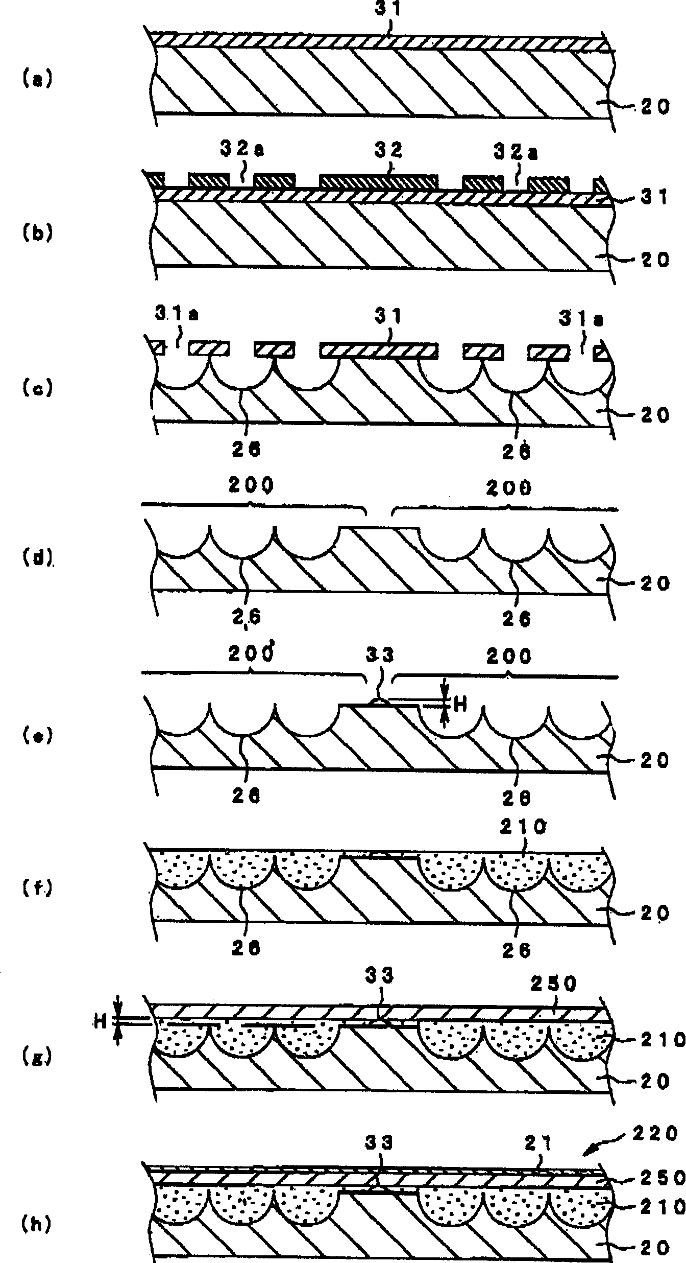
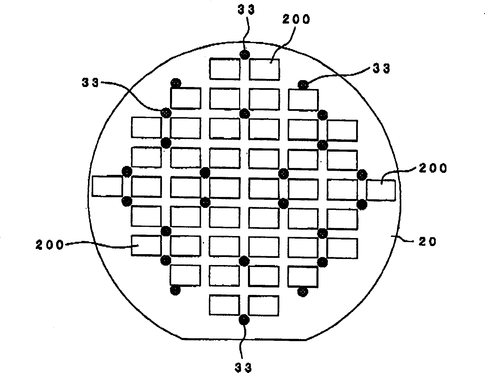
[0101] based on Figure 4 , Embodiment 1 of the method of dot-drawing the support body 33 on the lens glass substrate 20 will be specifically described. Figure 4 It is an enlarged cross-sectional view of a main part showing the drawing state of the support according to this embodiment.

[0102] In this embodiment, the curable material used as the molding material of the support body 33 is discharged from the droplet ejection device main body 300 to the surface of the lens glass substrate 20 in a predetermined amount, and when the curable material adheres to the lens glass substrate 20 Surface tension forms the support body 33 of height H.

[0103] Here, the configuration of the droplet discharge device main body 300 will be briefly described. The droplet discharge device main body 300 corresponds to a head body of an inkjet printer, and includes a piezoelectric element 301 constituting an ultrasonic wave generating unit. Electrodes (not shown) are provided on both surfaces...

Embodiment 2

[0116] based on Figure 5 , Embodiment 2 of the method of dot-drawing the support body 33 on the lens glass substrate 20 will be specifically described.

[0117]Although in the above-mentioned Embodiment 1, the height H of the support body 33 is set using the surface tension of the curable material, in this embodiment, the cured liquid mixed with the spacer 34 is discharged from the droplet discharge device main body 300 in a predetermined amount. The support body 33 is formed by drawing dots on the lens glass substrate 20 using a non-reactive material.

[0118] The curable material diluted with the solvent and the spacer 34 are supplied to the liquid agent storage portion 304 of the droplet discharge device main body 300 . The spacer 34 is made of glass fiber, glass beads, etc., and is a sphere with a particle diameter of 5 to 20 μm. In actual use, the particle diameter is determined according to the height H of the support body 33 .

[0119] Furthermore, in addition to the...

Embodiment 3

[0126] based on Figure 6 , Embodiment 3 of the method of dot-drawing the support body 33 on the lens glass substrate 20 will be specifically described.

[0127] Although in the above-mentioned second embodiment, the liquid solution mixed with the spacer 34 in the curable material is discharged from the droplet discharge device main body 300, and the support body 33 is formed on the lens glass substrate 20, but in this embodiment, the The spacer 34 is scattered on the lens glass substrate 20 , and then the support body 33 is dot-drawn on the lens glass substrate 20 with the curable material discharged from the droplet discharge device main body 300 . Therefore, only the curable material diluted with the solvent is discharged from the droplet discharge device main body 300 .

[0128] In this composition, first, if Figure 6 As shown in (a), spacers 34 are scattered throughout the lens glass substrate 20 . The particle size of the spacer 34 is determined by the height H of th...


PUM


Abstract

The invention aims at providing an electro-optical device which homogenizes the thickness of a micro lens layer and realizes the homogenization of the lens performance. A lens glass substrate (20) and a covering glass substrate (250) which are in mutually opposite direction and the micro lens layer (210) which is clamped between the substrates are arranged on a large opposite substrate (200). The thickness of the micro lens layer (210) is regulated by a bearing body (33) which is formed from solidified materials that are discharged from a droplet discharging device main body (300). Because the thickness of the micro lens layer (210) is regulated according to the bearing body (33), the thickness of the micro lens layer (210) can be homogenized.

Description

technical field [0001] The present invention relates to an electro-optical device in which a gap between a pair of opposing substrates is defined by a support formed of adhesive discharged from a droplet discharge device main body, a manufacturing method thereof, and an electronic device using the electro-optic device. Background technique [0002] Projection-type display devices such as liquid crystal projectors have a structure in which light irradiated from a light source is optically modulated by an electro-optic device serving as a light valve, and then enlarged and projected forward. As a liquid crystal device as an example of an electro-optical device, an active matrix type liquid crystal device is often used in order to improve display quality. [0003] In an active matrix liquid crystal device, pixels including pixel electrodes are formed in a matrix on the active matrix substrate side, and an active element such as a thin film transistor (TFT) is formed on each pix...

Claims


Application Information

Patent Timeline
IPC IPC(8): G02F1/133G02F1/1335
Inventor 铃木富雄
Owner SEIKO EPSON CORP
Learn More