Image sensor having a passivation layer exposing at least a main pixel array region and methods of fabricating the same
An image sensor and main pixel technology, applied in the field of image sensors, can solve problems such as the reduction of sensor sensitivity, and achieve the effect of eliminating the effects of absorption and refraction and making the image sensor sensitive.
- Summary
- Abstract
- Description
- Claims
- Application Information
AI Technical Summary
Problems solved by technology
Method used
Image
Examples
Embodiment Construction
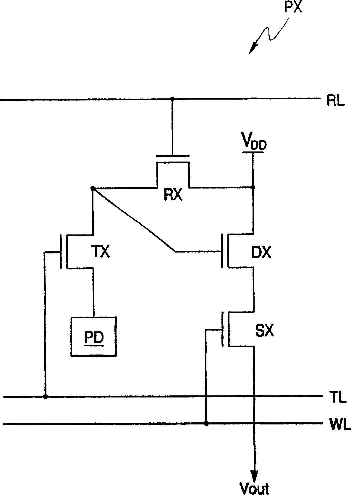
[0041] figure 2A schematic diagram comprising an active pixel PX according to the present invention. The active pixel PX includes a photodiode PD for capturing light and converting it into an electrical signal, ie a certain amount of charge. Transfer transistor TX receives charge from photodiode PD and transfers charge from the photodiode to the floating diffusion region of the pixel sensor circuit. A reset diode RX is used to reset any charge accumulated in the floating diffusion to a reference level. The driving transistor DX is connected in a source follower manner to buffer the output voltage Vout. The selection transistor SX is used during selection of the pixel circuit.
[0042] The gate electrode of the transfer transistor TX is electrically connected to the transfer line TL of the circuit. The gate electrode of the reforming transistor RX is electrically connected to the reset line RL. The gate electrode of the selection transistor SX is electrically connected to...
PUM
 Abstract
Description
Claims
Application Information


