Image sensor and methods of fabricating the same

An image sensor and main image technology, which is applied in the field of image sensors, can solve the problem of sensor sensitivity reduction and achieve the effect of eliminating absorption and refraction effects and sensitive image sensors

Active Publication Date: 2010-05-26
SAMSUNG ELECTRONICS CO LTD
View PDF4 Cites 0 Cited by
  • Summary
  • Abstract
  • Description
  • Claims
  • Application Information

AI Technical Summary

Problems solved by technology

Therefore, the sensitivity of the sensor decreases

Method used


Image

  • Image sensor and methods of fabricating the same
  • Image sensor and methods of fabricating the same
  • Image sensor and methods of fabricating the same

Examples


Embodiment Construction

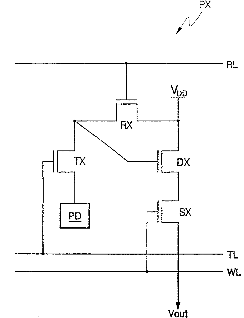
[0041] figure 2A schematic diagram comprising an active pixel PX according to the present invention. The active pixel PX includes a photodiode PD for capturing light and converting it into an electrical signal, ie a certain amount of charge. Transfer transistor TX receives charge from photodiode PD and transfers charge from the photodiode to the floating diffusion region of the pixel sensor circuit. A reset diode RX is used to reset any charge accumulated in the floating diffusion to a reference level. The driving transistor DX is connected in a source follower manner to buffer the output voltage Vout. The selection transistor SX is used during selection of the pixel circuit.

[0042] The gate electrode of the transfer transistor TX is electrically connected to the transfer line TL of the circuit. The gate electrode of the reforming transistor RX is electrically connected to the reset line RL. The gate electrode of the selection transistor SX is electrically connected to...


PUM


Abstract

The present invention concerns a CMOS image sensor with improved sensitivit. A CMOS image sensor with improved sensitivity includes a main pixel array region of an active pixel array region formed ona semiconductor substrate. A passivation layer is formed over the sensor, and it is at least partially removed from the main pixel array region, such that incident light being detected by the main pixel array does not pass through the passivation layer. Optical absorption and refraction caused by the material of the passivation layer are eliminated, resulting in an image sensor with improved optical sensitivity.

Description

technical field [0001] The present invention relates to image sensors, and more particularly to CMOS image sensors with improved sensitivity. Background technique [0002] An image sensor is a device that receives an optical signal from an object and converts the optical signal into an electrical signal. The electrical signal can then be transmitted for further processing, such as digitization, and then stored in a storage device such as a memory or an optical or magnetic disk, or for display on a display, printing, etc. Image sensors are commonly used in devices such as digital cameras, video cameras, printers, facsimile machines, and the like. [0003] Image sensors are generally of two types, charge coupled device (CCD) sensors and CMOS image sensors (CIS). CCD sensors generally have advantages including low noise operation and device uniformity. CIS devices are generally characterized by low power consumption and can operate at high speed due to high frame rate capabi...

Claims


Application Information

Patent Timeline
Patent Type & Authority Patents(China)
IPC IPC(8): H01L27/146H04N5/335
CPCH01L27/1462H01L27/14685H01L27/14627H01L27/14621H01L27/14645H01L27/14623H01L21/31H01L27/146
Inventor 朴永薰李受哲金起弘安正李容济裵贞勋黄圣仁安有真金范锡
Owner SAMSUNG ELECTRONICS CO LTD
Why Eureka
Try Eureka