Method of reilizing electromagnetic wave function appliance based on metal micro nano structure
A technology of functional devices and micro-nano structures, applied in the directions of instruments, optical components, installation, etc., can solve the problems of lack of degrees of freedom, inconcentration of near-field energy of outgoing light, deflection, splitting, and difficulty in focusing, etc.
- Summary
- Abstract
- Description
- Claims
- Application Information
AI Technical Summary
Problems solved by technology
Method used
Image
Examples
Embodiment 1
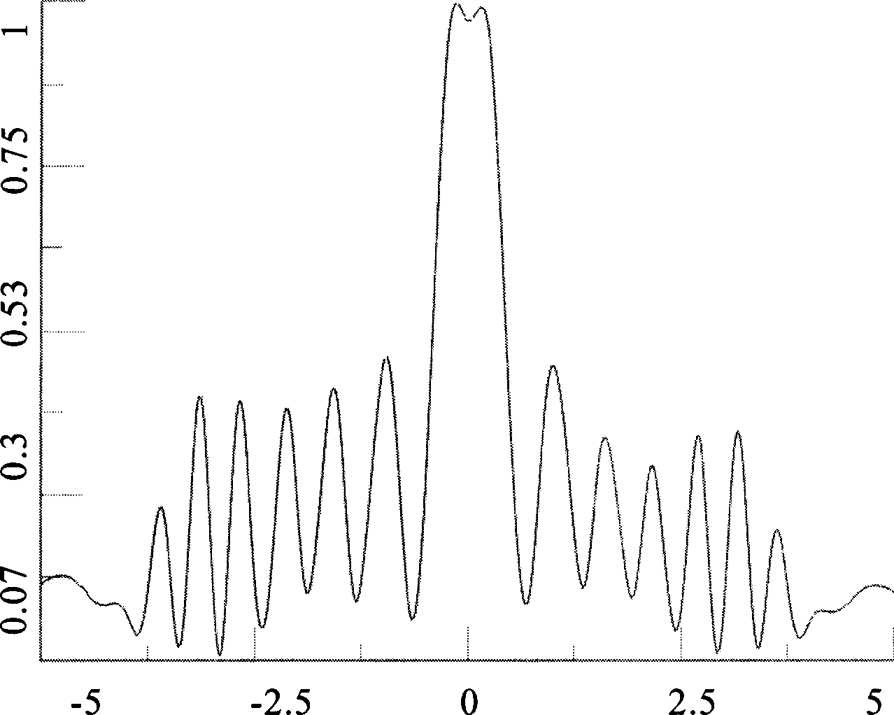
[0033] Embodiment 1, through the method of the present invention, the long focal depth of the plane wave and the concentrating effect of the submicron focal spot are realized, and the implementation process is as follows:
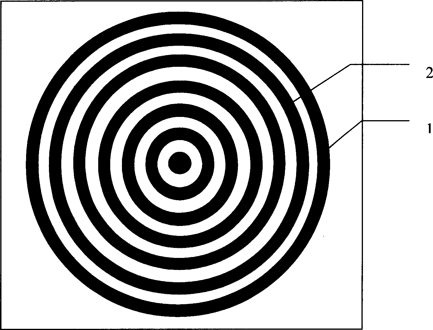
[0034](1) In this embodiment, the micro-nano structure needs to be used to realize the long-focus depth and sub-micron focal spot focusing effect of the plane light wave. Since the dielectric function of metal materials has different responses to incident light of different wavelengths, metallic silver Ag is selected as the metal material for the visible light band. slightly less than half a wavelength). According to the long focal depth effect of the element, the phase distribution of the light field exit surface of the element is obtained through the Huygens-Fresnel principle as follows: Figure 10 shown;
[0035] (2) With the optical axis of the micro-nano device as the center, a metal through hole is set, and according to the requirements of surface p...
Embodiment 2
[0039] Embodiment 2 is to realize the long focal depth of the plane wave and the submicron double-beam concentrating effect by the method of the present invention, and its implementation process is as follows:
[0040] (1) In this embodiment, the micro-nano structure needs to be used to realize the long-focus depth of the plane light wave and the sub-micron double-beam focusing effect. Since the dielectric function of metal materials has different responses to incident light of different wavelengths, silver is also selected as the metal material for the visible light band. Firstly, 300nm metallic silver is vapor-deposited on the surface of the quartz substrate, and the phase distribution of the light field on the exit surface is calculated as Figure 11 distributed.
[0041] (2) With the optical axis of the micro-nano device as the center, a plurality of grooves are arranged on both sides or around the through hole. According to the double-beam concentrating effect that need...
PUM
| Property | Measurement | Unit |
|---|---|---|
| radius | aaaaa | aaaaa |
Abstract
Description
Claims
Application Information


