

Luminous element with high light enucleation efficiency
A technology for light-emitting components and extraction efficiency, which is applied to electrical components, semiconductor devices, circuits, etc., can solve the problems of increasing the manufacturing complexity and cost of light-emitting diodes, and cannot effectively overcome the light absorption effect of semiconductor stacks.
- Summary
- Abstract
- Description
- Claims
- Application Information
AI Technical Summary
Problems solved by technology
Method used
Image

Examples
Embodiment 1
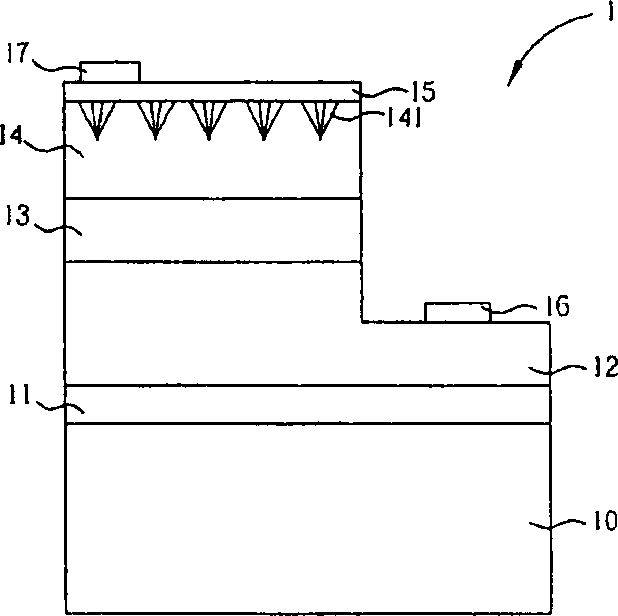
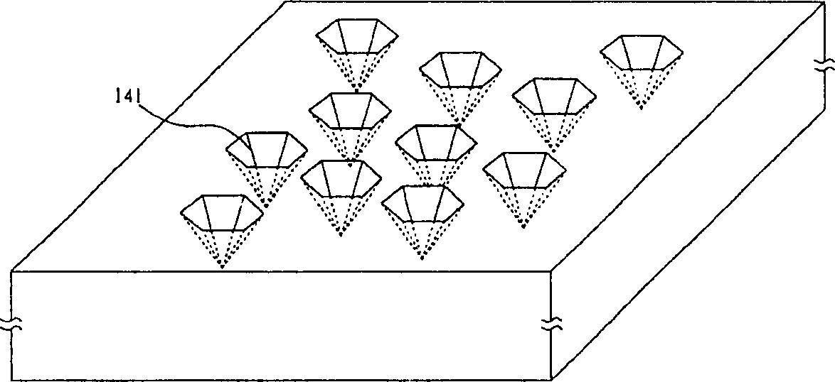
[0033] see figure 1 According to a preferred embodiment of the present invention, a light-emitting element 1 with high light extraction efficiency includes a sapphire substrate 10; a nitride buffer layer 11 formed on the sapphire substrate; an N-type nitride buffer layer formed on the nitride buffer layer 11 Nitride semiconductor stack 12, wherein the N-type nitride semiconductor stack 12 includes a first surface and a second surface away from the nitride buffer layer; a nitride multiple quantum well formed on the first surface emits light Layer 13; a P-type nitride semiconductor stack 14 formed on the nitride multiple quantum well light-emitting layer, and the surface of the P-type nitride semiconductor stack 14 away from the nitride multiple quantum well light-emitting layer includes a plurality of downward extending Inner hexagonal cone-shaped hole structure 141; a transparent conductive layer 15 formed on the P-type nitride semiconductor stack 14, wherein, the surface of t...
Embodiment 2
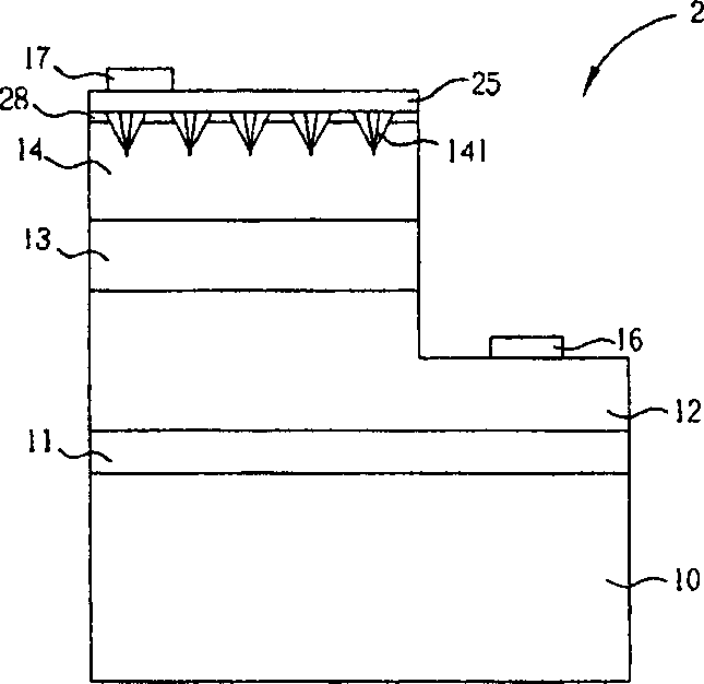
[0036] According to another embodiment of the present invention, it has a similar structure to Embodiment 1, and the difference is that the inner hexagonal cone hole structure is in the P-type semiconductor stack, and the inner hexagonal cone hole starting layer is a The epitaxial temperature ranges from 700°C to 950°C to change the epitaxial nucleation form, and form an inner hexagonal cone hole structure in the P-type semiconductor stack or surface layer. The size and density of the inner hexagonal cone-shaped holes can be controlled by controlling the change of the epitaxial temperature and the rate of temperature rise and fall, thereby changing the light extraction efficiency.
Embodiment 3
[0038] According to another embodiment of the present invention, it has a similar structure to Embodiment 1, and the difference is that the inner hexagonal cone hole structure is in the P-type semiconductor stack, and the inner hexagonal cone hole starting layer is a Nitrogen-rich atmosphere for epitaxial growth, so that it changes the epitaxial nucleation form, and is formed in the P-type semiconductor stack or surface layer. By adjusting the ratio of nitrogen gas, hydrogen gas and nitrogen reaction source in the epitaxial atmosphere, the size and density of the inner hexagonal cone-shaped holes can be adjusted, thereby changing the light extraction efficiency.
PUM
| Property | Measurement | Unit |
|---|---|---|
| thickness | aaaaa | aaaaa |
| depth | aaaaa | aaaaa |
Abstract
Description
Claims
Application Information