Novel surface roughening method for GaN-based light emitting diode

A technology of light-emitting diodes and surface roughening, which is applied in the direction of electrical components, circuits, semiconductor devices, etc., can solve the problems of increasing the complexity of existing processes, the difficulty of obtaining mask materials, and the lack of commercialization, etc., and achieves low cost and easy Clean, easily repeatable results

Inactive Publication Date: 2013-10-30
江门市奥伦德光电有限公司
View PDF5 Cites 5 Cited by
  • Summary
  • Abstract
  • Description
  • Claims
  • Application Information

AI Technical Summary

Problems solved by technology

These methods have problems such as difficult acquisition of mask materials, lack of commercialization and complicated post-processing, increasing the complexity of existing processes, etc.

Method used


Image

  • Novel surface roughening method for GaN-based light emitting diode
  • Novel surface roughening method for GaN-based light emitting diode

Examples


Embodiment 1

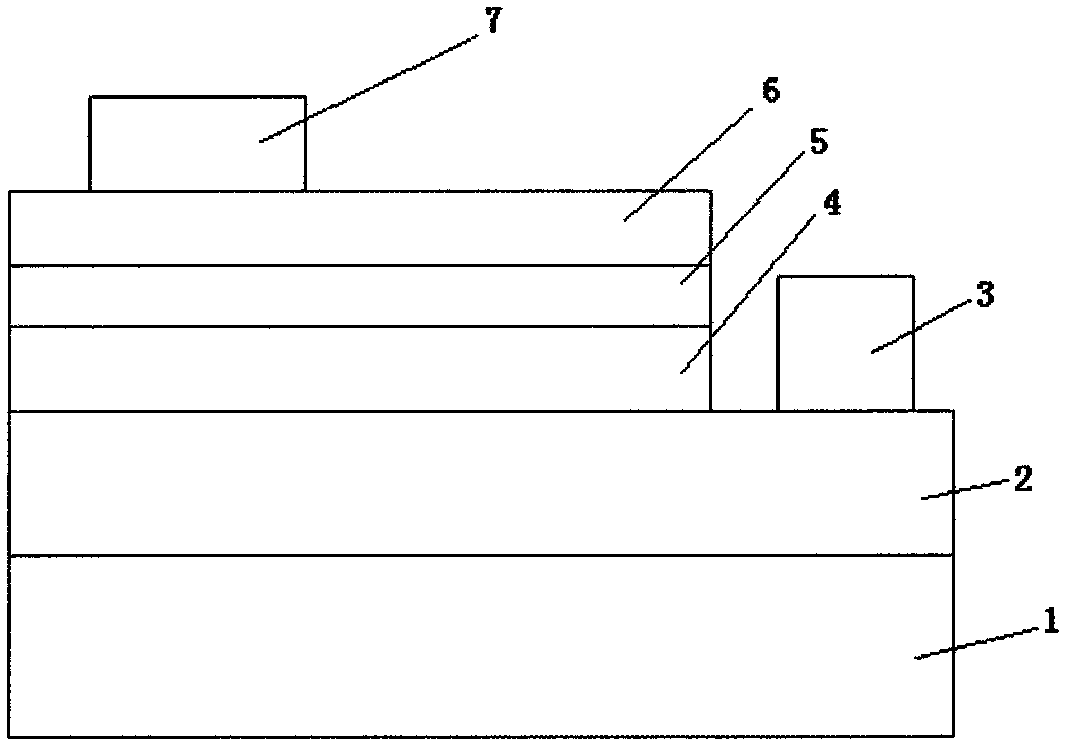
[0029] Embodiment 1, at first, on sapphire substrate 1, grow n-type semiconductor layer sequentially by MOCVD method

[0030] 2. The light emitting layer 4 and the p-type semiconductor layer 5 that control the light emitting wavelength. GaN epitaxial wafers were obtained after annealing. The above methods for forming GaN-based epitaxial wafers are well known to those skilled in the art to which the present invention belongs, and thus will not be described in detail.

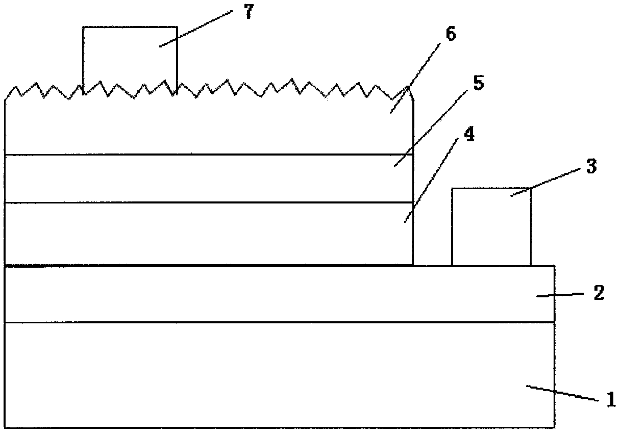
[0031] A current spreading layer (transparent electrode layer ITO) 6 is vacuum evaporated on the epitaxial wafer with a thickness of 1000-6000A and an evaporation temperature of 100-700°C. Uniformly disperse a layer of SiO with a diameter of 300nm on the transparent electrode by spin coating 2 nanosphere solution. The solution is dried at a temperature of 50-500° C., followed by ICP dry etching, and the etching time is 10-500 seconds. Finally, the SiO was washed off with hydrofluoric acid solution 2 Nanosphe...

Embodiment 2

[0033] In Embodiment 2, first, an n-type semiconductor layer 2 , a light-emitting layer 4 for controlling the light-emitting wavelength, and a p-type semiconductor layer 5 are sequentially grown on a silicon substrate 1 by MOCVD method. GaN epitaxial wafers were obtained after annealing. The above methods for forming GaN-based epitaxial wafers are well known to those skilled in the art to which the present invention belongs, and thus will not be described in detail.

[0034] A current spreading layer (transparent electrode layer) 6 is vacuum evaporated on the epitaxial wafer with a thickness of 1000-6000A and an evaporation temperature of 100-700°C. Uniformly disperse a layer of SiO with a diameter of 300nm on the transparent electrode by spin coating 2 nanosphere solution. The solution is dried at a temperature of 50-500° C., followed by ICP dry etching, and the etching time is 10-500 seconds. Finally, the SiO was washed off with hydrofluoric acid solution 2 Nanospheres f...

Embodiment 3

[0036] Embodiment 3, at first, on sapphire substrate 1 by MOCVD method, grow n-type semiconductor layer sequentially

[0037] 2. The light emitting layer 4 and the p-type semiconductor layer 5 that control the light emitting wavelength. GaN epitaxial wafers were obtained after annealing. The above methods for forming GaN-based epitaxial wafers are well known to those skilled in the art to which the present invention belongs, and thus will not be described in detail.

[0038] A current spreading layer (transparent electrode layer) 6 is vacuum evaporated on the epitaxial wafer with a thickness of 1000-6000A and an evaporation temperature of 100-700°C. Uniformly disperse a layer of SiO with a diameter of 600 nm on the transparent electrode by spin coating 2 nanosphere solution. The solution is dried at a temperature of 50-500° C., followed by ICP dry etching, and the etching time is 10-500 seconds. Finally, the SiO was washed off with hydrofluoric acid solution 2 Nanospheres...


PUM


Abstract

The invention relates to a novel surface roughening method for a GaN-based light emitting diode and the method is capable of improving light extraction efficiency. The method comprises the steps of growing N-type GaN material, a light emitting active layer and P-type GaN material on a substrate; depositing a layer of P-type transparent electrode used for ohmic contact on P-type material; preparing a layer of SiO2 nanospheres on the transparent electrode; taking the SiO2 nanospheres as a mask etching P-type transparent electrode, cleaning and removing residual SiO2 nanospheres and obtaining a LED device with a roughened light emitting surface. According to the invention, light extraction efficiency of the diode can be effectively improved. In addition, preparation method is simple, process is easy to control, and therefore the novel surface roughening method for the GaN-based light emitting diode is suitable for mass production with no special requirements for growth equipment and process conditions.

Description

technical field [0001] The invention relates to a surface treatment method, in particular to a novel GaN-based light-emitting diode surface roughening method. technical background [0002] At present, under the background of the increasingly serious problem of global warming, saving energy and reducing greenhouse gas emissions has become an important issue faced by the whole world. A low-carbon economy based on low energy consumption, low pollution, and low emissions will become an important direction of economic development. In the lighting field, semiconductor light-emitting products represented by LED (light-emitting diode) have the advantages of energy saving, environmental protection, long light source life and small size, and are attracting the attention of the world. [0003] The current conventional structure of gallium nitride-based light-emitting diodes includes a first type of N-type semiconductor layer, an active layer for controlling the emission wavelength, a ...

Claims


Application Information

Patent Timeline
Patent Type & Authority Applications(China)
IPC IPC(8): H01L33/38
Inventor 郝锐马学进吴质朴
Owner 江门市奥伦德光电有限公司
Why Eureka
Try Eureka