A method and apparatus for forming a high quality low temperature silicon nitride layer

A technology of silicon nitride layer and nitrogen source is applied in the fields of forming transistor dielectric layers, processing substrates, and forming silicon nitride layers, and can solve the problems of low density, difficult to control particle formation, and poor film quality.

Inactive Publication Date: 2006-02-08
APPLIED MATERIALS INC
View PDF1 Cites 54 Cited by
  • Summary
  • Abstract
  • Description
  • Claims
  • Application Information

AI Technical Summary

Problems solved by technology

Disilane and hexachlorodisilane have weak Si-Si bonds, which make it possible to obtain acceptable deposition rates, but when used with nitrogen sources such as ammonia, they either lead to poor film quality (low density and high hydrogen content , poor step coverage and microloading, for disilane), or lead to almost uncontrollable particle formation phenomena (for hexachlorodisilane)

Method used


Image

  • A method and apparatus for forming a high quality low temperature silicon nitride layer
  • A method and apparatus for forming a high quality low temperature silicon nitride layer
  • A method and apparatus for forming a high quality low temperature silicon nitride layer

Examples


Embodiment Construction

[0018] The present invention relates to the formation of high quality silicon nitride layers that can be formed at reduced or low deposition temperatures. In the following description, numerous specific details are set forth, such as deposition and annealing equipment, in order to provide a thorough understanding of the present invention. However, one of ordinary skill in the art will recognize that the present invention may be practiced without these specific details. In other instances, well-known semiconductor processing techniques have not been described in detail in order not to obscure the present invention.

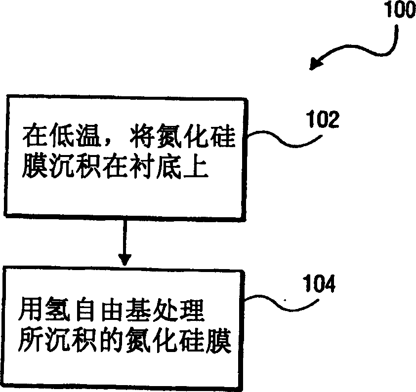
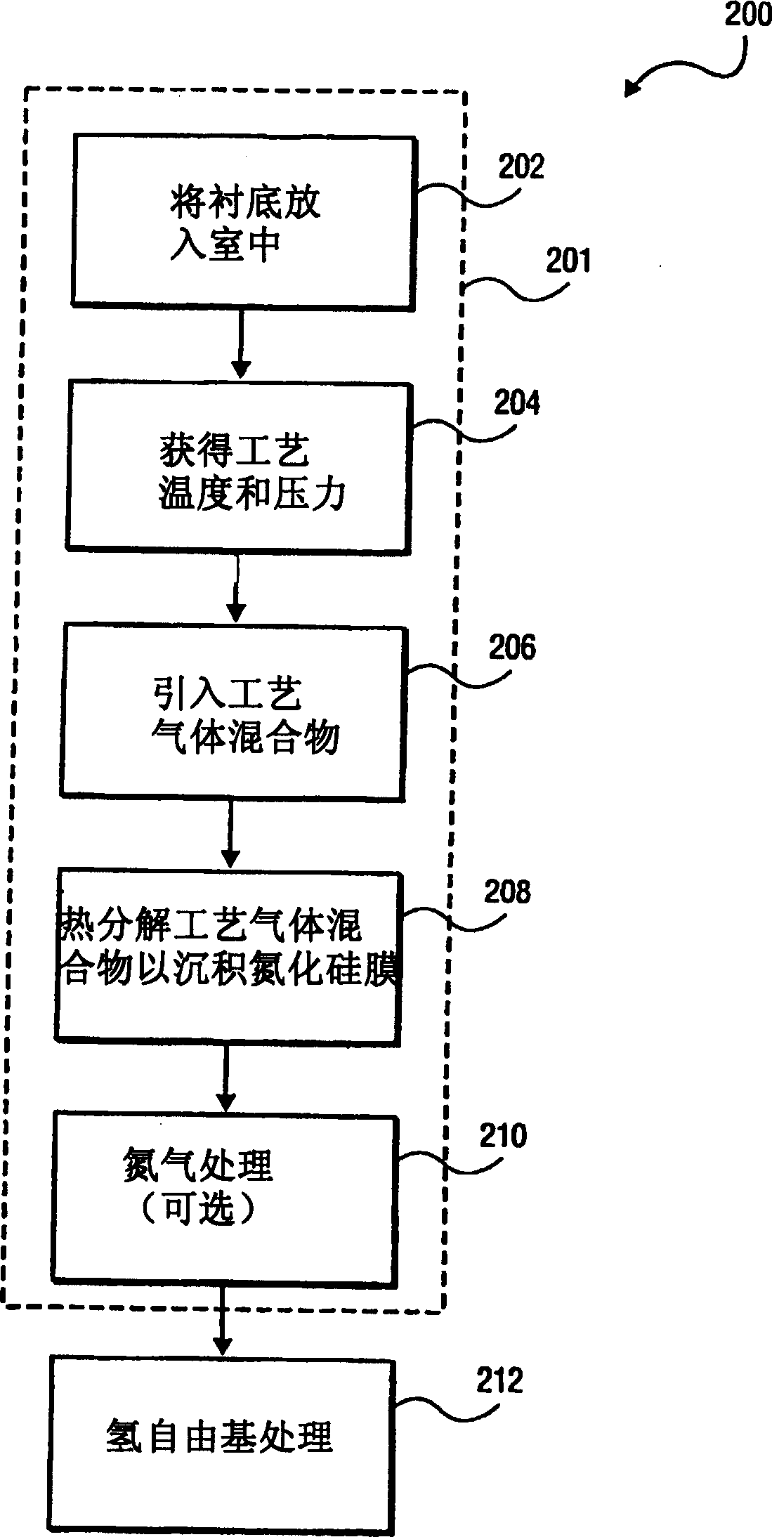
[0019] The present invention provides methods and apparatus for forming high quality silicon nitride layers by thermal chemical vapor deposition (CVD) at low deposition temperatures below 550°C. An example of a method of depositing a silicon nitride layer is in figure 1 A general description is given in the flowchart of . According to the first step of the prese...


PUM

PropertyMeasurementUnit
refractive indexaaaaaaaaaa

Abstract

A method of forming a silicon nitride layer is described. According to the present invention, a silicon nitride layer is deposited by thermally decomposing a silicon / nitrogen containing source gas or a silicon containing source gas and a nitrogen containing source gas at low deposition temperatures (e.g., less than 550 DEG C) to form a silicon nitride layer. The thermally deposited silicon nitride layer is then treated with hydrogen radicals to form a treated silicon nitride layer.

Description

Background of the invention [0001] The present invention relates to the field of thin layer formation, and more particularly, the present invention relates to methods and apparatuses for forming silicon nitride layers. [0002] Related Technical Discussions [0003] Modern integrated circuits consist of millions of transistors integrated into functional circuits. In order to further improve the computing power and storage capacity of integrated circuits, transistor feature dimensions, such as gate length and gate oxide film thickness, must be further scaled down. However, as transistor gate lengths are continuously scaled down, the electrical characteristics and performance of the transistors can vary greatly due to thermal redistribution of dopants in the device. Likewise, as devices are further scaled down, the thermal budget used to fabricate integrated circuits, ie, the individual process and cumulative heat inputs from deposition and process temperatures, must also be r...

Claims


Application Information

Patent Timeline
Patent Type & Authority Applications(China)
IPC IPC(8): C23C16/34C23C16/56H01L21/30
Inventor S・王E・A・C・桑柴兹A・(史蒂文)・陈
Owner APPLIED MATERIALS INC
Why Eureka
Try Eureka