Integrated circuit packaging structure and manufacturing method thereof

A technology of integrated circuit and packaging structure, which is applied to the application of carbon nanotube array heat conduction integrated circuit packaging structure and its manufacturing field, which can solve the problems of unfavorable popularization and application, complicated manufacturing and packaging process, poor thermal conductivity, etc., and achieve excellent thermal conductivity performance, uniform heat dissipation, and improved efficiency

Inactive Publication Date: 2006-02-15
HONG FU JIN PRECISION IND (SHENZHEN) CO LTD +1
View PDF2 Cites 10 Cited by
  • Summary
  • Abstract
  • Description
  • Claims
  • Application Information

AI Technical Summary

Problems solved by technology

However, the semiconductor packaging structure based on this thermal interface material has disadvantages. First, due to the poor thermal conductivity of the polymer matrix material, the thermal interface material formed by mixing carbon nanotubes with the polymer matrix cannot fully utilize the carbon nanotubes. The thermal conductivity of nanotubes, and the thermal interface material will cause uneven heat conduction due to the uneven heating of the chip during application, which will affect the thermal conduction efficiency and stability of the entire thermal interface material, and further affect the packaging structure. second, the thermal interface material that mixes the carbon nanotube array in the polymer matrix in the above-mentioned semiconductor packaging structure is formed on the integrated circuit chip (DIE), because the integrated circuit chip cannot withstand the required heat for forming the carbon nanotube array. High temperature, so it is necessary to form the carbon nanotube array thermal interface material on the substrate in advance, and then fabricate the integrated circuit chip on the substrate. The manufacturing and packaging process is relatively complicated, which is not conducive to popularization and application.

Method used


Image

  • Integrated circuit packaging structure and manufacturing method thereof
  • Integrated circuit packaging structure and manufacturing method thereof
  • Integrated circuit packaging structure and manufacturing method thereof

Examples


Embodiment Construction

[0039] The present invention will be described in detail below in conjunction with the accompanying drawings and specific embodiments.

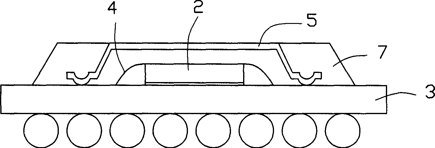
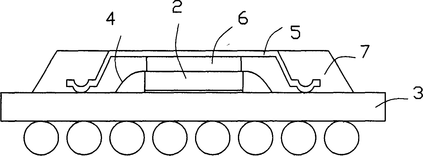
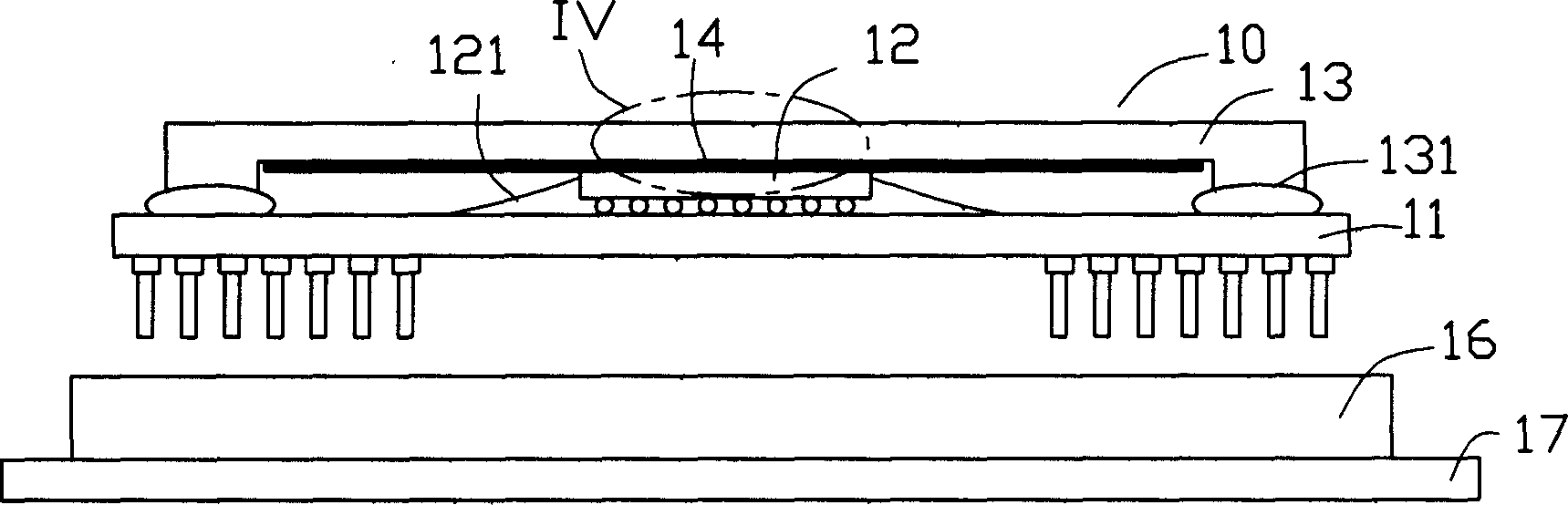
[0040] see image 3 and Figure 4The present invention provides an integrated circuit packaging structure 10, which includes: a substrate 11; an integrated circuit chip (DIE) 12 bonded on the substrate 11, and electrically connected to the substrate through a gold wire 121; an integrated heat sink ( Integrated Heat Spreader (IHS) 13 is arranged above the integrated circuit chip 12, and this integrated heat sink 13 includes an inner surface and an outer surface, and its edge lower end 131 is bonded on the substrate 11, and this integrated heat sink plays sealing and protection The role of the integrated circuit chip 12, meanwhile, the lower end 131 of the edge of the integrated heat sink 13 is electrically connected to the ground electrode of the substrate 11 through a circuit, and plays the role of electrostatic shielding; a carbon nanotube ...


PUM


Abstract

The IC package structure comprises a base plate, an IC on base plate, an integrated heat sink plate composed of inner and outer surfaces that is arranged on top of IC chip with edge lower end fixed on base, and a carbon nano pipe array formed on the said inner surface with two ends vertical contact to integrated heat sink plate and IC chip; wherein, there is nano metal material of high thermal conductivity filled in the said pipe.

Description

【Technical field】 [0001] The invention relates to an integrated circuit packaging structure and a manufacturing method thereof, in particular to an integrated circuit packaging structure using a carbon nanotube array for heat conduction and a manufacturing method thereof. 【Background technique】 [0002] In the field of packaging of semiconductor integrated circuits, with the continuous improvement and development of semiconductor integrated circuits, their functions continue to increase while their volumes continue to decrease, their density continues to increase, and their packaging sizes continue to decrease. Since the integrated circuit chip performs calculation and processing in such a small space when it is working, it will inevitably generate a considerable amount of heat. The generated heat must be dissipated in an appropriate way to avoid calculation and processing errors due to overheating of the integrated circuit chip, and in severe cases, damage to the hardware c...

Claims


Application Information

Patent Timeline
Patent Type & Authority Applications(China)
IPC IPC(8): H01L23/433H05K7/20H01L21/50
CPCH01L2224/16227H01L2224/73204H01L2224/73253H01L2924/15311H01L2924/15312H01L2924/16251
Inventor 吕昌岳余泰成黄全德黄文正林志泉陈杰良
Owner HONG FU JIN PRECISION IND (SHENZHEN) CO LTD
Why Eureka
Try Eureka