
Laser induced thermal imaging apparatus

An imaging device and laser technology, applied in lighting devices, optics, light sources, etc., can solve problems such as reduced luminous efficiency and lifespan, and reduced lifespan of organic layers.

Active Publication Date: 2006-03-08
SAMSUNG DISPLAY CO LTD
View PDF1 Cites 0 Cited by
  • Summary
  • Abstract
  • Description
  • Claims
  • Application Information

AI Technical Summary

Problems solved by technology

That is, when the organic layer is exposed to oxygen or water vapor, the lifetime of the organic layer is reduced, or when the organic layer includes an emissive layer, its luminous efficiency and lifetime are reduced

Method used


Image

  • Laser induced thermal imaging apparatus
  • Laser induced thermal imaging apparatus
  • Laser induced thermal imaging apparatus

Examples


Embodiment Construction

[0022] Hereinafter, the present invention will be described more fully with reference to the accompanying drawings showing preferred embodiments of the invention. However, the present invention may be embodied in different forms and should not be construed as limited to the embodiments set forth in this application. On the contrary, these embodiments are provided to make the technical solutions disclosed in this application more sufficient and complete, and enable those skilled in the art to more fully understand the technical scope claimed by the present invention. In the drawings, the thicknesses of layers and regions are exaggerated for clarity. Throughout the specification, the same symbols refer to the same elements.

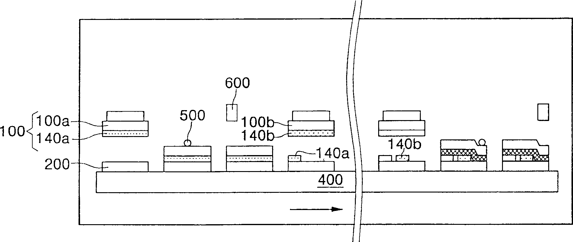
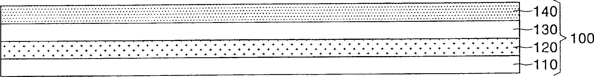
[0023] Figure 1A with Figure 1B is a cross-sectional view of a LITI device according to an embodiment of the present invention.

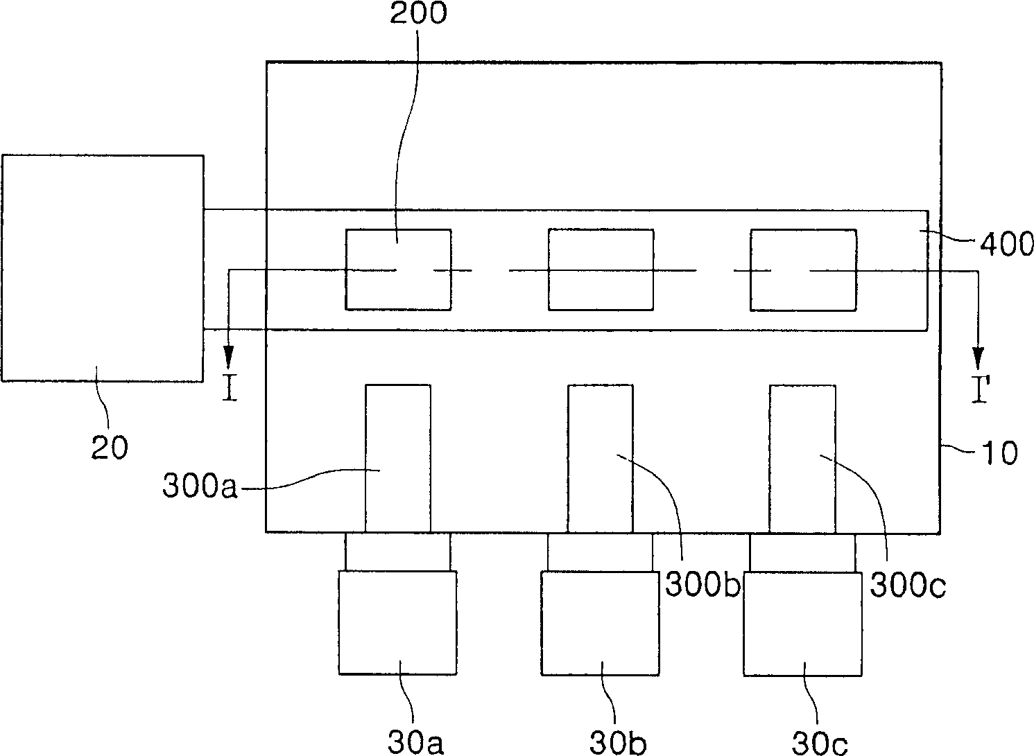
[0024] refer to Figure 1A , there is a platform 400 inside the chamber 10 , the substrate 200 is placed on the platform 4...


PUM


Abstract

A laser induced thermal imaging apparatus for fabricating an organic light emitting display is provided. The laser induced thermal imaging apparatus includes a stage where a substrate is positioned; a transport device for transporting a donor substrate; a laminator for laminating the substrate to the donor substrate; a laser optical unit for performing the LITI, and a chamber supplied with an atmospheric pressure of an inert gas in which the stage, the laminator, and the laser optical unit are positioned.

Description

[0001] This application claims the priority of Korean Patent Application No. KR2004-68758 filed on August 30, 2004, the entire disclosure of which is hereby incorporated by reference. technical field [0002] The invention relates to a laser induced thermal imaging apparatus, in particular to a laser induced thermal imaging apparatus used for manufacturing an organic light emitting display. Background technique [0003] Generally among flat-panel displays, organic light-emitting displays (OLEDs) have a fast response speed of less than 1 ms, low power consumption, and are emissive displays, so that there is no viewing angle problem, and they are used to display moving pictures regardless of size The display medium will be more advantageous. In addition, it can be manufactured at low temperature and the process of manufacturing organic light-emitting displays based on conventional semiconductor process technology is also simple, making it considered as a next-generation flat p...

Claims


Application Information

Patent Timeline
Patent Type & Authority Applications(China)
IPC IPC(8): H05B33/10H05B33/14B41J2/435B41M5/26G03F3/10H01L27/32H01L51/40H01L51/56
CPCH01L51/56B41J2/325H01L51/0013B41M5/38221H10K71/18H10K71/421H10K71/50H10K71/00
Inventor 金茂显陈炳斗宋明原李城宅
Owner SAMSUNG DISPLAY CO LTD
Features
  • Generate Ideas
  • Intellectual Property
  • Life Sciences
  • Materials
  • Tech Scout
  • Unparalleled Data Quality
  • Higher Quality Content
  • 60% Fewer Hallucinations
Learn More