Method for forming electronic devices in multi-layer structure of substrate

A technology for electronic devices and multi-layer structures, which is applied in the fields of electro-solid devices, nanotechnology for information processing, nanotechnology for materials and surface science, etc. It can solve the problems of insufficient position accuracy and small overlapping capacitance.

Inactive Publication Date: 2010-06-09
PLASTIC LOGIC LTD
View PDF5 Cites 1 Cited by
  • Summary
  • Abstract
  • Description
  • Claims
  • Application Information

AI Technical Summary

Problems solved by technology

Furthermore, the positional accuracy of drop placement in techniques such as direct inkjet printing is often insufficient to obtain small overlapping capacitances

Method used


Image

  • Method for forming electronic devices in multi-layer structure of substrate
  • Method for forming electronic devices in multi-layer structure of substrate
  • Method for forming electronic devices in multi-layer structure of substrate

Examples


Embodiment Construction

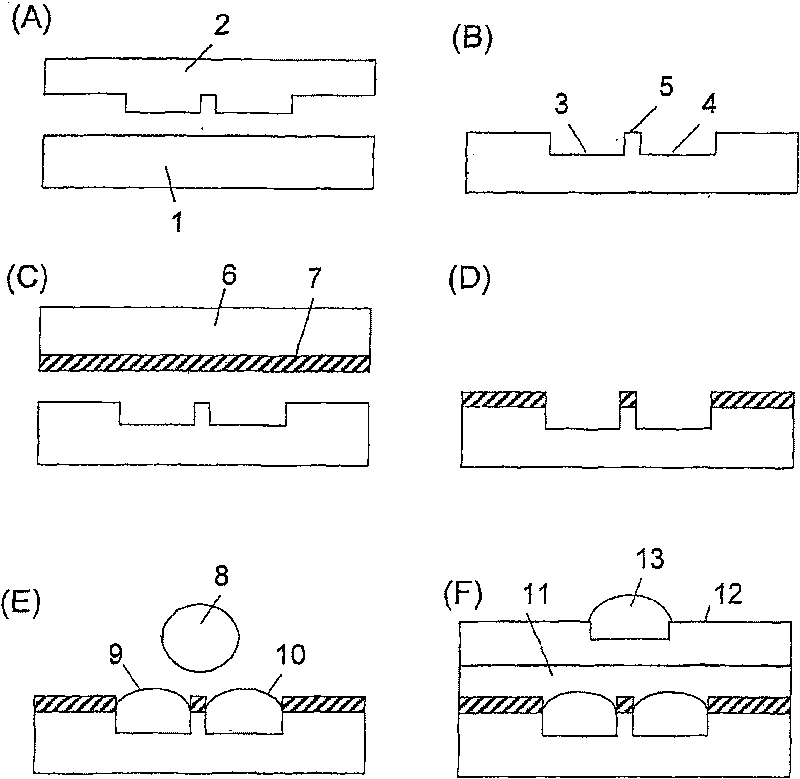
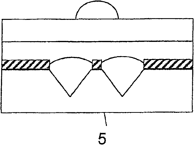
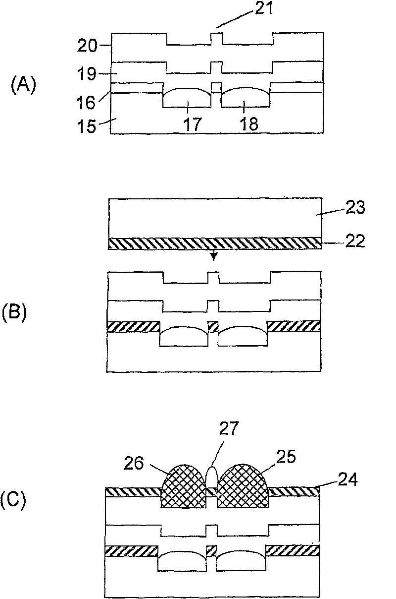
[0026] figure 1 A schematic diagram showing the use of imprinting to define the critical channel length of a FET device. The substrate 1 is a flexible plastic substrate such as poly(ethylene terephthalate) (PET), polyethersulfone (PES), and polyethylene naphthalate (PEN). Alternatively, the substrate may be a rigid substrate, such as a glass substrate coated with a polymer layer. The substrate is imprinted by pressing an embossing tool 2 comprising an array of raised features into the substrate. The imprinting step is performed at an elevated temperature, preferably close to the glass transition temperature of the substrate or the uppermost layer on the substrate. The embossing step can also be carried out by placing the substrate 1 in its liquid phase. Preferably, the thickness of the polymer layer is chosen to be greater than the height of the raised features of the embossing tool. If the polymer layer is thinner than the height of the raised features of the stencil, car...


PUM

PropertyMeasurementUnit
thicknessaaaaaaaaaa
thicknessaaaaaaaaaa
glass transition temperatureaaaaaaaaaa

Abstract

A method for forming an electronic device in a multilayer structure comprising the steps of: defining a topographic profile in a laterally extending first layer; depositing at least one non-planarizing layer on top of the first layer such that the topographic profile of the surface of the or each non-planarizing layer conforms to that of the laterally extending first layer; and depositing a pattern of at least one additional layer onto the top-most non-planarizing layer, such that the lateral location of the additional layer is defined by the shape of the topographic profile of the non-planarizing layer, and whereby the additional layer is laterally aligned with the topographic profile in the first layer.

Description

technical field [0001] The present invention relates to electronic devices, particularly organic electronic devices, and methods of forming the devices. Background technique [0002] Recently, semiconducting conjugated polymer thin-film transistors (TFTs) have been investigated for inexpensive logic circuits integrated on plastic substrates (C. Drury et al., APL 73, 108 (1998)) and high-resolution active-matrix Optoelectronic integrated devices and pixel transistor switches in displays (H. Sirringhaus et al., Science 280, 1741 (1998), A. Dodabalapur et al., Appl. Phys. Lett. 73, 142 (1998)). High performance TFTs have been demonstrated in test device configurations with polymer semiconductor and inorganic metal electrodes and gate dielectric layers. Carrier mobility as high as 0.1 cm2 / Vs and ON-OFF (on-off) current ratio of 106-108 have been achieved, which are comparable to the performance of amorphous silicon TFTs (H. Sirringhaus et al., Advance in Solid State Physics 39...

Claims


Application Information

Patent Timeline
Patent Type & Authority Patents(China)
IPC IPC(8): H01L51/05H01L51/40H01L21/762H01L51/00H01L51/10H01L51/30
CPCH01L51/0022B82Y10/00H01L51/0525H01L51/0039B05D5/12H01L51/0023H01L51/057H01L51/0021H01L51/0036H01L51/0017H01L2251/105B05D1/322H01L51/052B05D3/145H01L51/0043H01L51/0037H01L51/0545Y10S977/887H01L51/105H01L51/0541H01L51/0016B82Y30/00H10K71/221H10K71/231H10K71/611H10K71/60H10K71/621H10K85/115H10K85/1135H10K85/113H10K85/151H10K10/472H10K10/471H10K10/491H10K10/464H10K10/84H10K10/466H10K71/821
Inventor 托马斯·M.·布朗汉宁·司瑞英豪司
Owner PLASTIC LOGIC LTD
Why Eureka
Try Eureka