

Method and equipment for fabricating structure of compound crystal
A manufacturing method and flip chip technology, applied in microstructure devices, measurement devices, semiconductor/solid-state device manufacturing, etc., can solve problems such as high equipment costs, impact on product yield, and clean room costs.
- Summary
- Abstract
- Description
- Claims
- Application Information
AI Technical Summary
Problems solved by technology
Method used
Image

Examples
Embodiment Construction
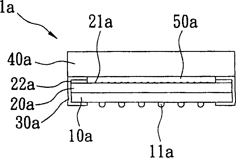
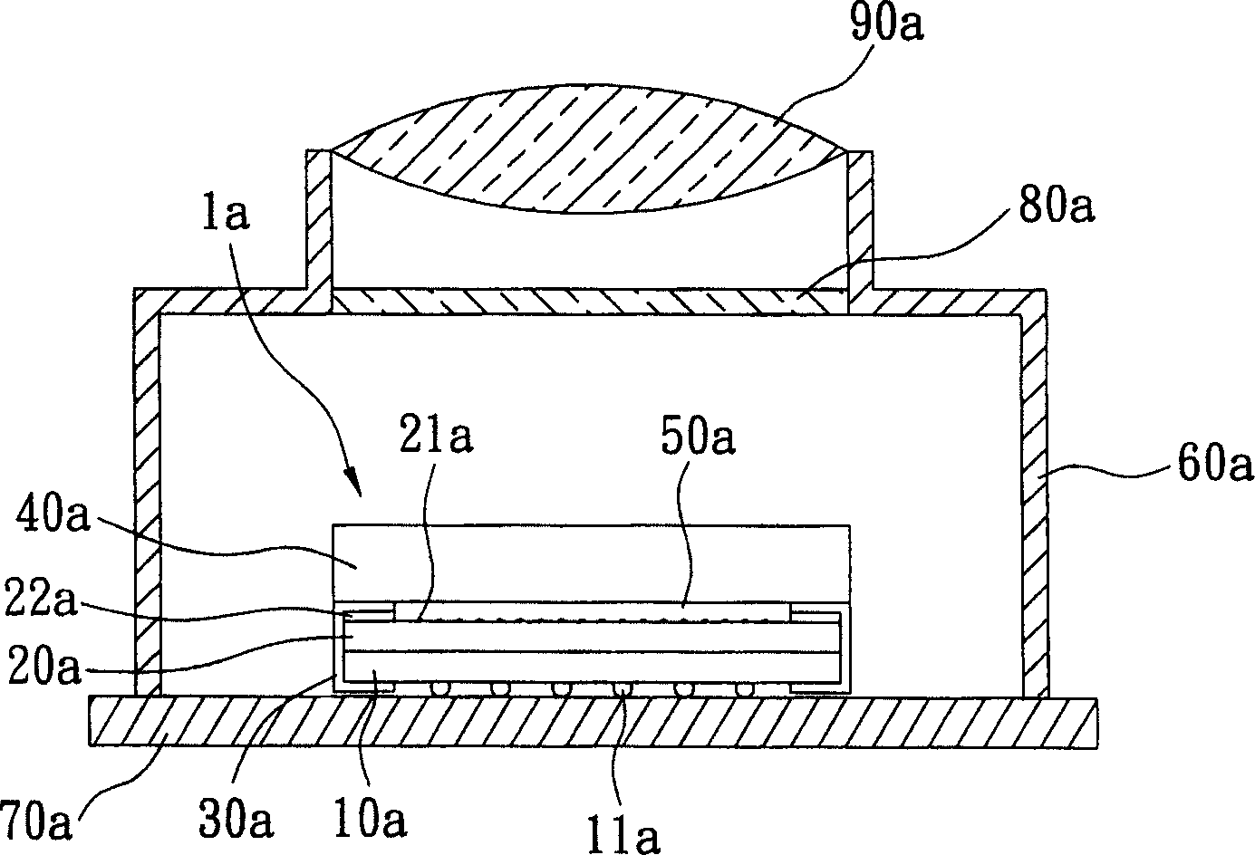
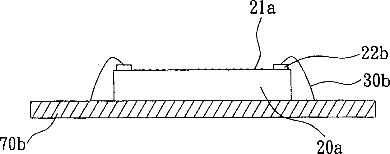
[0046] See Figure 3 with Figure 4A to Figure 4F First obtain a transparent substrate 10, then bond the chip 20 to the transparent substrate 10, cooperate with the pre-arranged circuit layout layer 12 of the transparent substrate 10 to be electrically connected to the chip 20, and make sure that the inside is sealed and formed without being protected from the outside world. Interfering airtight interlayer 40 to form a so-called flip-chip device; the empty interlayer 40 is used to improve the image sensitivity of the flip-chip device; in addition, the transparent substrate 10 of the present invention has the circuit layout The layer 12 and the chip 20 are combined through the bonding pad 30, and at the same time have the functions of a circuit carrier and isolating dust; after completing the above simple steps, you can leave the excellent clean room to enter the subsequent process, such as for each The chip structure is cut into a single body, and can be assembled into a module...
PUM
 Abstract
Description
Claims
Application Information