

Method of manufacturing organic electroluminescent device and organic electroluminescent device
An electroluminescence device and a technology for a manufacturing method, which are applied in the manufacture of organic electroluminescence devices and the field of organic electroluminescence devices, can solve the problems of generating non-light-emitting regions, unable to obtain light-emitting characteristics and light-emitting life, and achieve improved accuracy and Effects of degrees of freedom
Active Publication Date: 2006-04-26
SEIKO EPSON CORP
View PDF4 Cites 18 Cited by
- Summary
- Abstract
- Description
- Claims
- Application Information
AI Technical Summary
Problems solved by technology
[0011] However, the inventors of the present invention have confirmed that even if the technology described in the above-mentioned patent documents is adopted, even if a buffer layer is provided, sufficient light-emitting characteristics and light-emitting life cannot be obtained, and non-light-emitting regions and the like are generated.
Method used
View moreImage
Smart ImageViewing Examples

Examples
Embodiment
[0298] Hereinafter, the present invention will be described more specifically by way of examples.
Login to View More PUM
| Property | Measurement | Unit |
|---|---|---|
| Viscosity at room temperature | aaaaa | aaaaa |
| Viscosity at room temperature | aaaaa | aaaaa |
| Film thickness | aaaaa | aaaaa |
Abstract
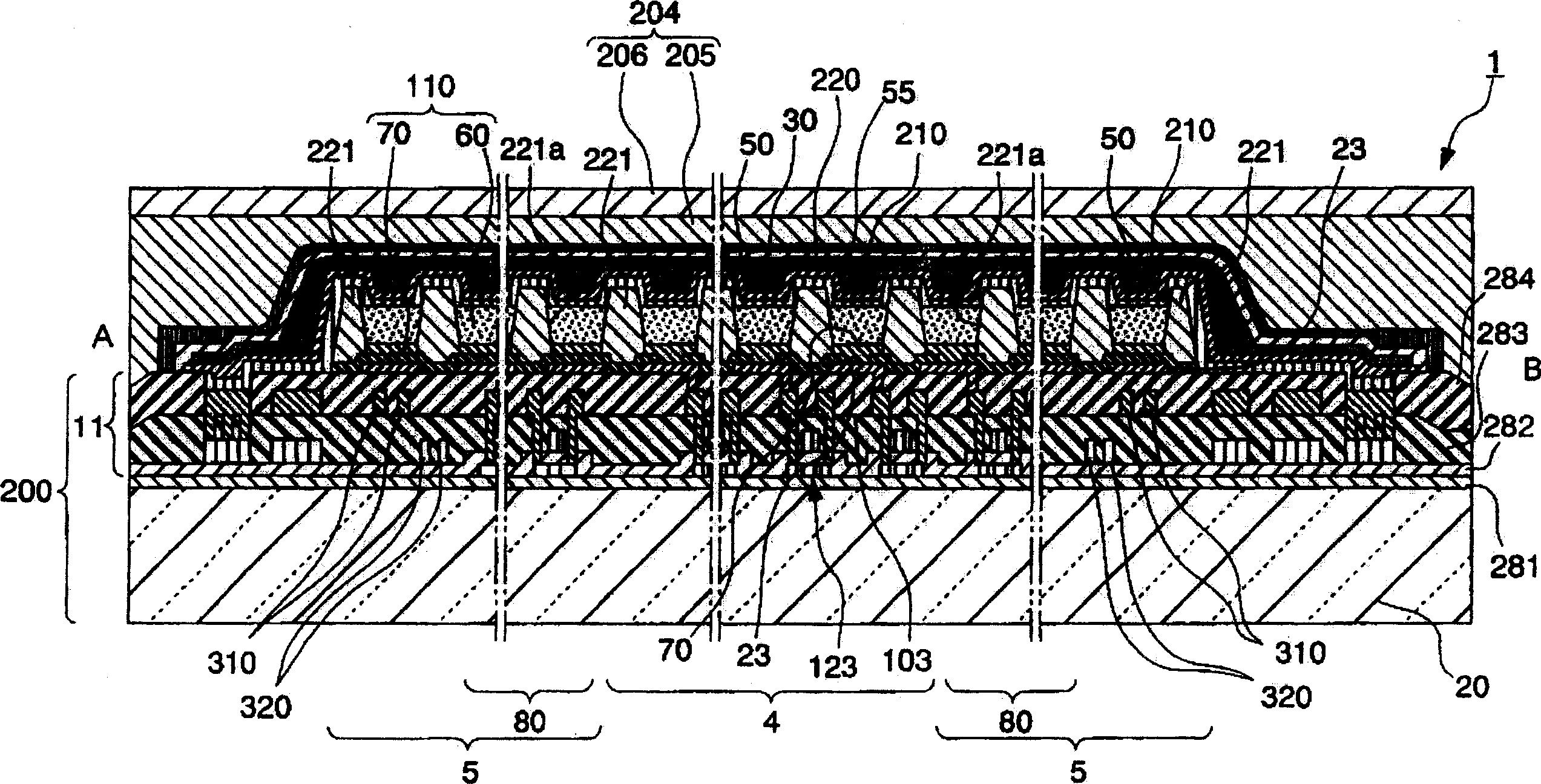
The invention provides a method for manufacturing an organic electroluminescent device, comprising a plurality of first electrodes on a substrate (20), a light-emitting functional layer arranged correspondingly to the formation positions of the first electrodes, and a layer covering the light-emitting function. A method for manufacturing an organic electroluminescent device for a second electrode of the layer, comprising: a buffer layer forming step of forming a buffer layer (210) while covering the second electrode; and forming a buffer layer (210) covering the second electrode. The process of the gas barrier layer ( ) 30, the buffer layer forming process includes: a coating process of coating a coating material having a monomer / oligomer material and a curing agent without using a solvent under a vacuum atmosphere, and making the coating material The thermal curing process of curing to form a buffer layer. According to the method of manufacturing an organic EL device of the present invention, sufficient luminescence characteristics or luminescence lifetime can be obtained and generation of non-luminescence regions can be suppressed. The present invention also provides an organic electroluminescent device.
Description
technical field [0001] The present invention relates to a method for manufacturing an organic electroluminescent device and an organic electroluminescent device. Background technique [0002] In recent years, an organic electroluminescent device (hereinafter, referred to as an organic EL device) having a light-emitting functional layer has been known. Such an organic EL device generally has an organic light-emitting layer between an inorganic anode and an inorganic cathode. Furthermore, in order to improve the hole injection property or electron injection property, a configuration in which an organic hole injection layer is arranged between an inorganic anode and an organic light-emitting layer, or a configuration in which an electron injection layer is arranged between an organic light-emitting layer and an inorganic cathode has been proposed. . [0003] Here, the electron injection layer, which has material properties that easily release electrons, easily reacts with moi...
Claims
Login to View More Application Information
Patent Timeline
 IPC IPC(8): H05B33/10G09F9/30H01L21/00H01L23/00H01L29/04H05B33/04
CPCH10K59/8722H10K59/873H10K59/87H05B33/10H05B33/22H10K50/84H10K50/844H10K50/8426
Inventor林建二野泽陵一山内幸夫
OwnerSEIKO EPSON CORP