Driving method, device of on-chip micro-nano object based on light force, and application

A driving method and driving device technology, applied in the field of light control, can solve the problems of easy pollution of the reaction field and poor controllability, and achieve the effects of improving the degree of accuracy, the degree of freedom, and the large control range.

Active Publication Date: 2021-10-22
WESTLAKE UNIV
View PDF3 Cites 0 Cited by
  • Summary
  • Abstract
  • Description
  • Claims
  • Application Information

AI Technical Summary

Problems solved by technology

[0005] The object of the present invention is to provide a driving method, device and application of on-chip micro-nano objects based on optical force, which can be based on optical force in a non-liquid environment Drive the on-chip micro-nano objects, and solve the problems of poor controllability of the existing on-chip micro-nano object drive transportation, and the reaction field in the liquid environment is easily polluted, so as to realize the controllability of micro-nano objects on the integrated chip Translation, swing, transport and release

Method used


Image

  • Driving method, device of on-chip micro-nano object based on light force, and application
  • Driving method, device of on-chip micro-nano object based on light force, and application
  • Driving method, device of on-chip micro-nano object based on light force, and application

Examples


preparation example Construction

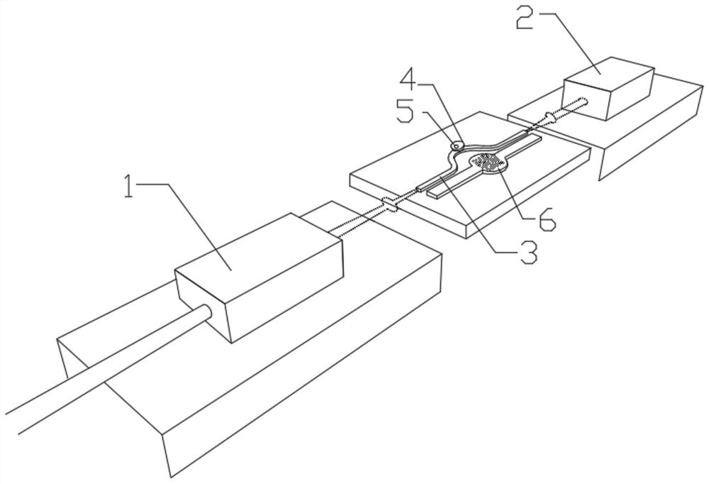
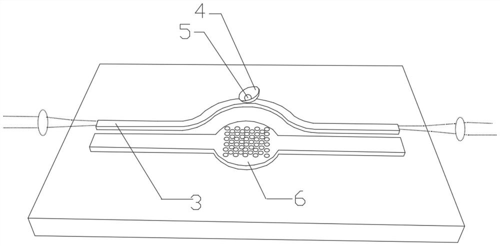
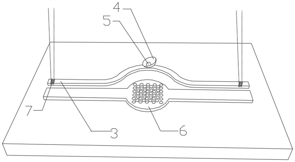
[0057] In the second aspect, this solution provides a method for preparing an on-chip micro-nano object driving device based on optical force, including the following steps: preparing an on-chip waveguide 3; preparing a micro-nano container 4 on the on-chip waveguide 3; using a probe to drive The micro-nano object 5 is transferred into the micro-nano container 4; the laser is coupled to the on-chip waveguide 3.

[0058] In the preparation scheme, the on-chip waveguide 3 can be prepared by using micro-nano processing and etching technology, and the micro-nano container 4 can be prepared on the on-chip waveguide 3 by using the micro-nano processing method and focused ion beam technology. The driven micro-nano object 5 is transferred into the micro-nano container 4. If the driven micro-nano object 5 is on the nanoscale, it can be transferred by using the micro-nano object 5 of the manipulator in the electron microscope.

[0059] In the third aspect, this solution provides an opti...

Embodiment 1

[0079] Embodiment 1: Translational drive of on-chip micro-nano objects based on optical force:

[0080] Place the object to be transported in the micro-nano container, fix the single pulse energy of the pulse laser 1 at 0.1-1 nanojoule at the initial stage, slowly increase the repetition frequency of the pulse light, so that the micro-nano container moves on the on-chip waveguide 3, wherein The initial position of point A, point B is the position corresponding to the movement time t1, and point C is the position corresponding to the movement time 10t1. Here, the repetition rate of the pulsed laser 1 can also be kept fixed, and the energy of a single pulse can be slowly increased. When the single pulse energy exceeds the threshold corresponding to driving the micro-nano container, the moving speed of the sample is proportional to the repetition frequency of the incident pulse laser and the single pulse energy.

[0081] Such as Figure 4 As shown, the micro-nano container move...

Embodiment 2

[0082] Embodiment 2: Swing drive of on-chip micro-nano objects based on optical force:

[0083] When the micro-nano-container 4 is transported to the target position of the waveguide, turn off the pulse laser and turn on the continuous laser. At this time, the translation of the sample stops and starts to swing. The frequency of the swing is the same as the modulation frequency of the continuous laser, and the amplitude of the swing is the same as that of the continuous laser. The power is proportional to the power, the greater the power, the greater the swing. Here, state C is the state before the continuous laser is turned on, and state D is the state after the continuous laser is turned on. When the swing speed is very high and exceeds the centrifugal force of the object being transported, the sample will break away from the micro-nano container, and the reached position can be precisely controlled by the swing speed.


PUM


Abstract

The invention provides a driving method and device of an on-chip micro-nano object based on light force and application. According to the scheme, a micro-nano container is placed on an on-chip waveguide, a micro-nano object is placed in the micro-nano container, and translation, swing and transportation of the micro-nano container are achieved through conversion of light energy and mechanical energy. According to the scheme, the on-chip micro-nano object can be driven based on light force in a non-liquid environment, and the problems that the controllability of existing on-chip micro-nano object driving transportation is poor, and a reaction field in the liquid environment is prone to being polluted are solved in a targeted mode.

Description

technical field [0001] The present invention relates to the field of light control, in particular to a driving method and system based on light energy-mechanical energy conversion to realize the transportation of on-chip micro-nano objects, which has important application prospects in on-chip laboratories and targeted delivery systems. Background technique [0002] As semiconductor integration technology shifts to a 28nm line width process, the research on semiconductor integration technology has also begun to enter the nanometer field. Correspondingly, the laboratory on a chip has emerged as the times require. Research on tiny sheets of glass, silicon, or plastic, such as semiconductor integrated circuits, of a few square centimeters. Due to its small size, the laboratory on a chip has many advantages such as microquantization of samples, high-speed reaction and analysis, etc., and is widely used in many fields such as disease diagnosis and treatment, drug screening, gene s...

Claims


Application Information

Patent Timeline
IPC IPC(8): G02B6/26G02B6/35
CPCG02B6/26G02B6/3536
Inventor 唐伟伟仇旻方啸国严巍
Owner WESTLAKE UNIV
Why Eureka
Try Eureka