Non-volatile memory and its manufacturing method and operating method

A non-volatile storage and non-volatile technology, applied in semiconductor/solid-state device manufacturing, electric solid-state devices, semiconductor devices, etc., can solve problems such as the inability to increase the integration of components and the large size of the programmable read-only memory storage unit

Inactive Publication Date: 2006-05-10
POWERCHIP SEMICON CORP
View PDF1 Cites 2 Cited by
  • Summary
  • Abstract
  • Description
  • Claims
  • Application Information

AI Technical Summary

Problems solved by technology

[0005] However, the above-mentioned SONOS device with a split gate structure has a larger memory cell size because the split gate structure requires a larger split gate area, so its memory cell size is smaller than that of the electrically erasable device with stacked gates. Moreover, the storage unit size of the programmable read-only memory is large, so the so-called problem that the integration degree of the components cannot be increased

Method used


Image

  • Non-volatile memory and its manufacturing method and operating method
  • Non-volatile memory and its manufacturing method and operating method
  • Non-volatile memory and its manufacturing method and operating method

Examples


Embodiment Construction

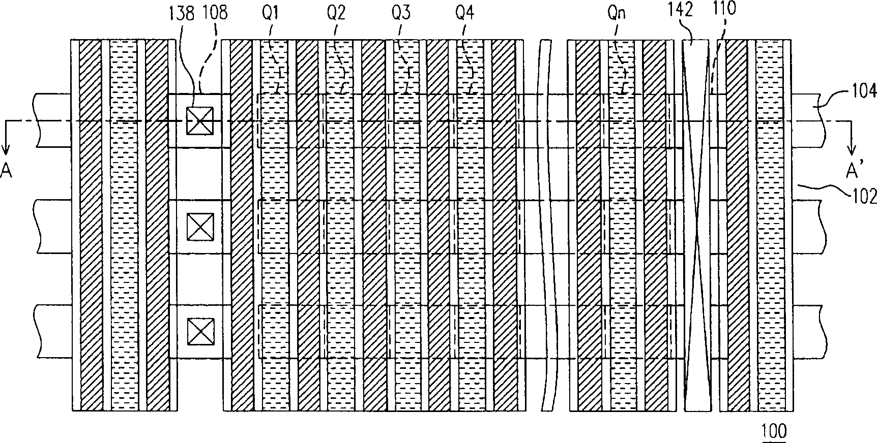
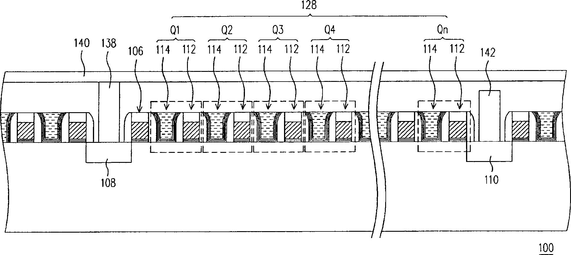
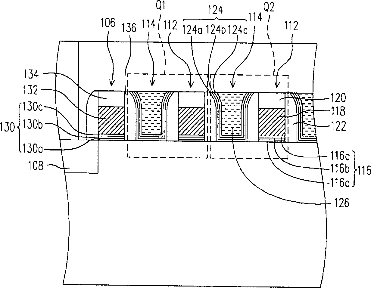
[0081] Figure 1A It is a top view showing a preferred embodiment of the non-volatile memory of the present invention. Figure 1B for illustration Figure 1A Structural cross-section along line A-A'. Figure 1C It is a cross-sectional view showing the structure of the storage unit and the selection unit of the present invention.

[0082] Please also refer to Figure 1A , Figure 1B and Figure 1C , the non-volatile memory structure of the present invention is at least composed of a substrate 100, an element isolation structure 102, an active region 104, a plurality of memory cells Q1-Qn, a selection unit 106, a drain region 108 (doped region), a source region 110 (doped region).

[0083]The substrate 100 is, for example, a silicon substrate, and the substrate 100 can be a P-type substrate or an N-type substrate. The device isolation structure 102 is disposed in the substrate 100 to define an active region 104 .

[0084] A plurality of memory cells Q1 -Qn are disposed on t...


PUM


Abstract

This invention relates to one fixed memory, which comprises multiple memory units formed by first and second units, wherein, The first memory unit is set on base; The second memory unit is set on the sidewall and base of the first memory unit; The first memory unit is formed by first grating electrode located between first grating electrode and base first compound medium layer; The second memory unit is formed by second grating electrode located between second grating electrode and base second compound medium layer; The second memory unit is isolated by first isolation gap wall and first memory unit, wherein, First compound medium layer and second layer are separately bottom medium layer, charge imbed layer and top medium layer.

Description

technical field [0001] The present invention relates to a semiconductor memory element, in particular to a non-volatile memory and its manufacturing method and operation method. Background technique [0002] Among all kinds of non-volatile memory products, it has the advantages of multiple data storage, reading, erasing, etc., and the stored data will not disappear after power off. Program read-only memory (EEPROM) has become a memory element widely used in personal computers and electronic equipment. [0003] A typical EEPROM uses doped polysilicon to make a floating gate and a control gate. Moreover, in order to avoid the problem of misjudgment of data due to excessive erasing phenomenon is too serious during erasing of typical electrically erasable and programmable read-only memory. A select gate is additionally provided on the sidewalls of the control gate, the floating gate, and the substrate to form a split-gate structure. [0004] In addition, in the prior art, a c...

Claims


Application Information

Patent Timeline
IPC IPC(8): H01L27/115H01L21/8247
Inventor 杨青松翁伟哲卓志臣
Owner POWERCHIP SEMICON CORP
Why Eureka
Try Eureka