Semiconductor laser unit and optical pickup device including the semiconductor laser unit
A laser and semiconductor technology, applied in the structural details of semiconductor lasers, semiconductor lasers, semiconductor devices, etc., can solve problems such as difficulty in ensuring positional accuracy, complicated operations, and complicated processes, and achieve thinning, easy assembly, and high heat dissipation efficiency. Effect
- Summary
- Abstract
- Description
- Claims
- Application Information
AI Technical Summary
Problems solved by technology
Method used
Image

Examples
Embodiment approach 1
[0056] First, refer to Figure 5 and Image 6 The semiconductor laser module of Embodiment 1 will be described.
[0057] Figure 5 It is an assembled perspective view of the semiconductor laser module of the first embodiment. Image 6 A is a plan view of the semiconductor laser module of Embodiment 1, Image 6 B is a side view of the semiconductor laser module of the first embodiment.
[0058] The semiconductor laser module of Embodiment 1 has a simple structure that is easy to assemble, heats up heat easily, and achieves high functionality and miniaturization.
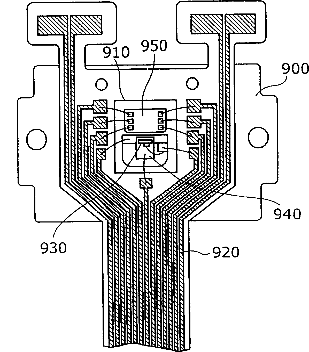
[0059] use Figure 5 The configuration of the semiconductor laser module according to Embodiment 1 will be described with respect to an assembled perspective view of FIG.
[0060] First, if Figure 5 As shown in A, an opening is provided in the center of a thin central portion (hereinafter referred to as "recess") 100a of the metal plate 100, and a flexible substrate 130 having a width wider than the width of t...
Embodiment approach 2
[0087] Next, refer to Figure 8 and Figure 9 A semiconductor laser module according to Embodiment 2 will be described.
[0088] Figure 8 It is an assembled perspective view of the semiconductor laser module of the second embodiment. Figure 9 A is a top view of the semiconductor laser assembly, Figure 9 B is a side view of the semiconductor laser assembly. and, with Figure 5 and Image 6 The same elements are assigned the same symbols, and detailed descriptions thereof are omitted.
[0089] In the semiconductor laser module of the second embodiment, as in the semiconductor laser module of the first embodiment, the thickness of the metal plate 100 (protrusion 100b and convex part 100c) in the region where the frame body 150 is provided is smaller than that of the silicon substrate 120. The thickness of the region (recess 100 a ) with the flexible substrate 130 is thick.
[0090] However, the semiconductor laser module of Embodiment 2 differs from the semiconductor l...
Embodiment approach 3
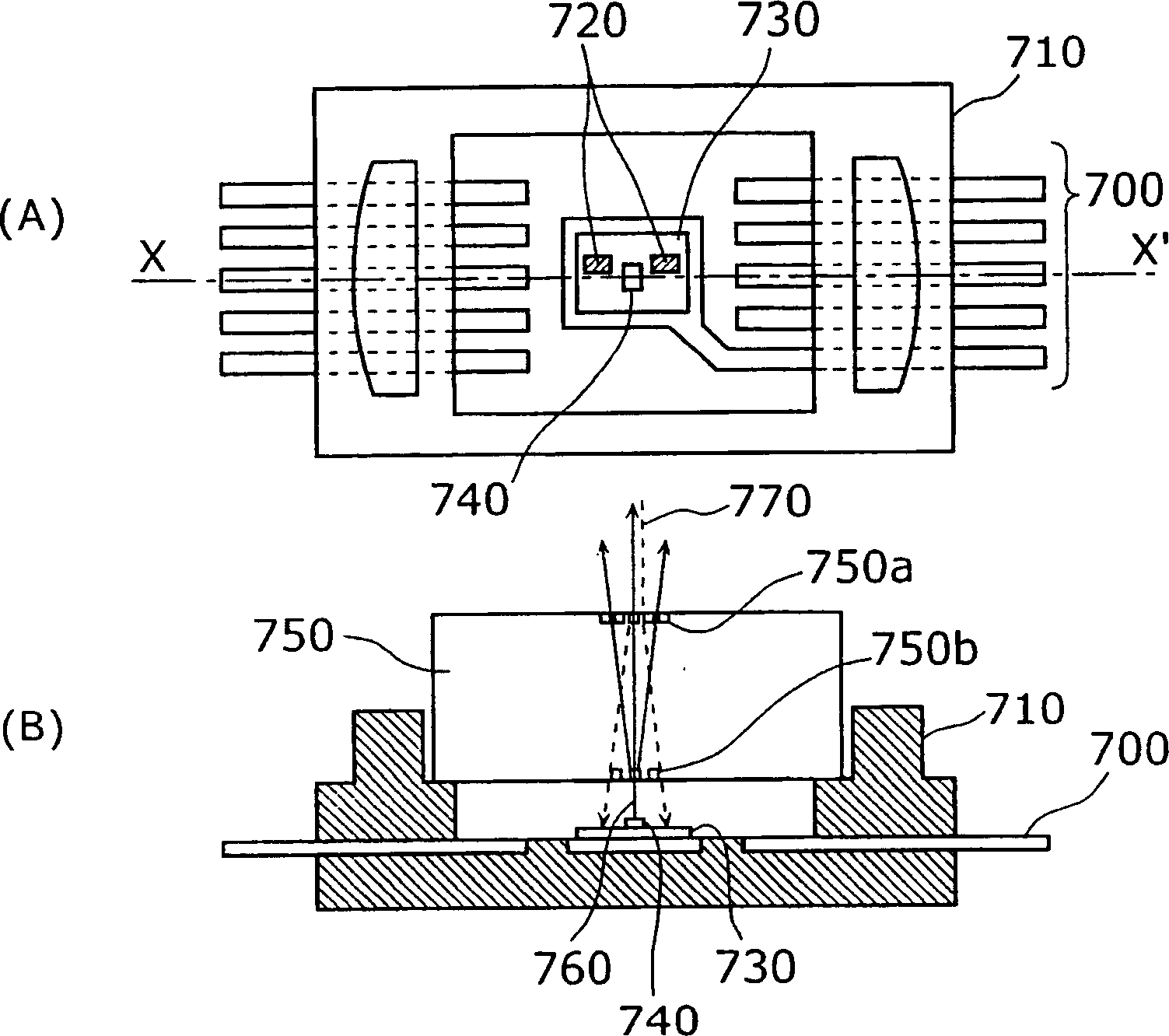
[0098] Next, refer to Figure 10 An optical pickup device according to Embodiment 3 will be described.
[0099] Figure 10 A is a plan view of an optical pickup device 600 according to Embodiment 3, Figure 10 B is a cross-sectional view of the optical pickup device 600 .
[0100] Optical pick-up device 600 is the device that reads data from optical disk 670, comprises: collimating lens 610, reflection mirror 620, object lens 630, semiconductor laser assembly 640 and heat dissipation block 650 of embodiment 1 or 2, and this heat dissipation block uses adhesive For example, a silicon-based thermally conductive adhesive is bonded and fixed to the back surface of the metal plate of the semiconductor laser module 640 .
[0101] The external optical pick-up device of the flexible substrate of the semiconductor laser assembly 640 is connected to the wiring of the flexible substrate, such as Figure 10 As shown in B, it is performed at the soldering place 660 outside the optical ...
PUM
 Abstract
Description
Claims
Application Information
 - R&D
- Intellectual Property
- Life Sciences
- Materials
- Tech Scout
- Unparalleled Data Quality
- Higher Quality Content
- 60% Fewer Hallucinations
Browse by: Latest US Patents, China's latest patents, Technical Efficacy Thesaurus, Application Domain, Technology Topic, Popular Technical Reports.
© 2025 PatSnap. All rights reserved.Legal|Privacy policy|Modern Slavery Act Transparency Statement|Sitemap|About US| Contact US: help@patsnap.com