Pixel circuit, display device, and a driving method thereof

A technology of pixel circuit and driving current, which is applied in the field of pixel circuit and can solve problems such as incorrectness

Inactive Publication Date: 2006-06-07
SONY CORP
View PDF5 Cites 4 Cited by
  • Summary
  • Abstract
  • Description
  • Claims
  • Application Information

AI Technical Summary

Problems solved by technology

Incidentally, since the threshold value of a P-channel transistor is negative,

Method used


Image

  • Pixel circuit, display device, and a driving method thereof
  • Pixel circuit, display device, and a driving method thereof
  • Pixel circuit, display device, and a driving method thereof

Examples


Embodiment Construction

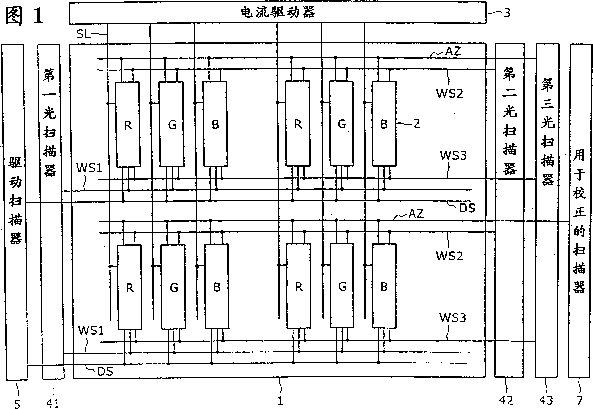
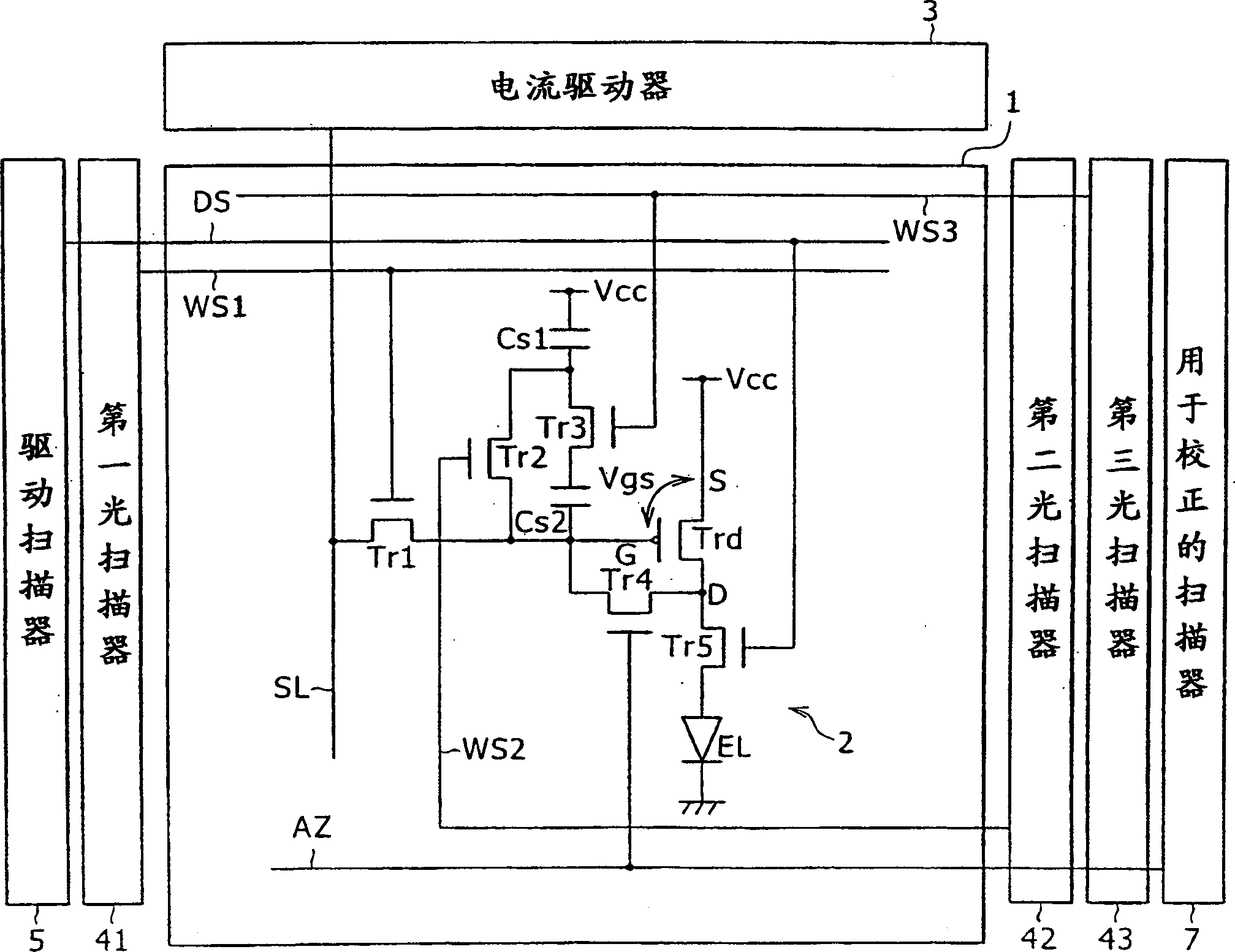
[0063] Preferred embodiments of the present invention will be described in detail below with reference to the accompanying drawings. FIG. 1 is a block diagram showing the overall structure of a display device according to an embodiment of the present invention. As shown in the figure, this display device is of an active matrix type, and is composed of a peripheral circuit portion and a pixel array 1 as a main portion. The peripheral circuit portion includes a current driver 3, a first optical scanner 41, a second optical scanner 42, a third optical scanner 43, a drive scanner 5, a scanner 7 for correction, and the like. The pixel array 1 is composed of pixels R, G, and B arranged in a matrix where the row-distributed wiring WS and the column-distributed signal line SL intersect with each other. Each pixel R, G, and B is constituted by a pixel circuit 2 . The signal line SL is driven by the current driver 3 . In other words, the current driver 3 alternately causes the signal...


PUM


Abstract

The invention discloses a pixel circuit arranged at a position where a signal line through which a signal current is forced to flow and a scanning line for supplying a control signal intersect with each other, the pixel circuit includes: an electroluminescent element; The electroluminescent element provides a driving transistor for driving current; and a control section adapted to operate according to the control signal to control the driving current of the driving transistor based on the signal current; the control section includes: a first sampling a unit for sampling a signal current caused to flow through the signal line; a second sampling unit for sampling a predetermined reference current caused to flow through the signal line just before or after the signal current and a difference unit, configured to generate a control voltage corresponding to the difference between the sampled signal current and the sampled reference current. The drive transistor receives the control voltage at its gate and supplies a drive current that is caused to flow through its source and drain to the electroluminescent element to cause the electroluminescent element EL to emit light.

Description

[0001] Related Application Cross Reference [0002] The present invention contains subject matter related to Japanese Patent Application JP 2004-347283 filed in the Japan Patent Office on Nov. 30, 2004, the entire content of which is hereby incorporated by reference. technical field [0003] The present invention relates to a pixel circuit arranged at each pixel for current driving of a corresponding electroluminescent element, and to a method for driving the pixel circuit. The present invention also relates to a display device having pixel circuits arranged in a matrix, and more particularly to controlling the amount of current flowing through an electroluminescent element such as an organic EL element by using an insulated gate field effect transistor provided in each pixel circuit A display device of the so-called active matrix type, and a method for driving the display device. Background technique [0004] In an image display device such as a liquid crystal display devi...

Claims


Application Information

Patent Timeline
IPC IPC(8): G09G3/30G09G3/20H05B33/14H05B44/00
CPCG09G3/3233G09G3/3241G09G3/325G09G2300/0417G09G2300/0819G09G2300/0852G09G2300/0861G09G2310/0262G09G2320/043G09G3/30G09G3/20
Inventor 山下淳一内野胜秀
Owner SONY CORP
Why Eureka
Try Eureka