Surface acoustic wave element and manufacturing method thereof

A surface acoustic wave and manufacturing method technology, applied in the direction of electrical components, impedance networks, etc., can solve problems such as difficulty in uniform thickness, steep passage characteristics, and inability to obtain stable frequency characteristics, and achieve the effect of stable frequency characteristics

Inactive Publication Date: 2006-06-07
SEIKO EPSON CORP
View PDF0 Cites 1 Cited by
  • Summary
  • Abstract
  • Description
  • Claims
  • Application Information

AI Technical Summary

Problems solved by technology

[0004] In such Non-Patent Document 1, the uppermost layer of the semiconductor wiring region and the SiO in the SAW region 2 The height of the layer is different, especially the uppermost layer of the semiconductor wiring area is lower than the SiO of the SAW area 2 The height above the layer, so in order to flatten the SiO in the SAW region where the IDT is formed 2 When the surface of the layer is polished by CMP (Chemical and Mechanical Polishing, chemical mechanical polishing), it is difficult to uniformly form SiO in the SAW region where the IDT is formed. 2 layer thickness
SiO in which the SAW region of the IDT is formed is known 2 Depending on the thickness of the layer, there is a difference in the speed of propagating sound waves (sonic speed), but since the frequency is proportional to the sound speed, when there are regions with different sound speeds in the same element, stable frequency characteristics and steep passage characteristics cannot be obtained. The problem

Method used


Image

  • Surface acoustic wave element and manufacturing method thereof
  • Surface acoustic wave element and manufacturing method thereof
  • Surface acoustic wave element and manufacturing method thereof

Examples


Embodiment approach 1

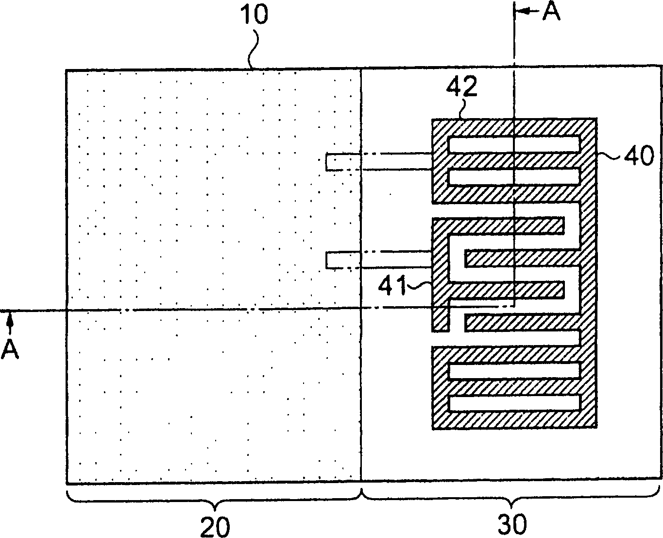
[0033] figure 1 It is a plan view showing the surface acoustic wave element of the first embodiment. exist figure 1In the surface acoustic wave element 10, the silicon layer 50 (refer to figure 2 ), the semiconductor wiring region 20 and the SAW region 30 are arranged side by side in the same plane. In the semiconductor wiring region 20, four layers of metal wiring (not shown) are formed (see figure 2 ). In addition, a comb-shaped IDT 40 is formed on the uppermost layer of the SAW region 30 .

[0034] The IDT 40 is composed of A1, has an input-side electrode 41 and an output-side electrode 42 inserted into each other, has terminals for input or output, respectively, and these terminals are connected to predetermined metal wirings not shown in the semiconductor region.

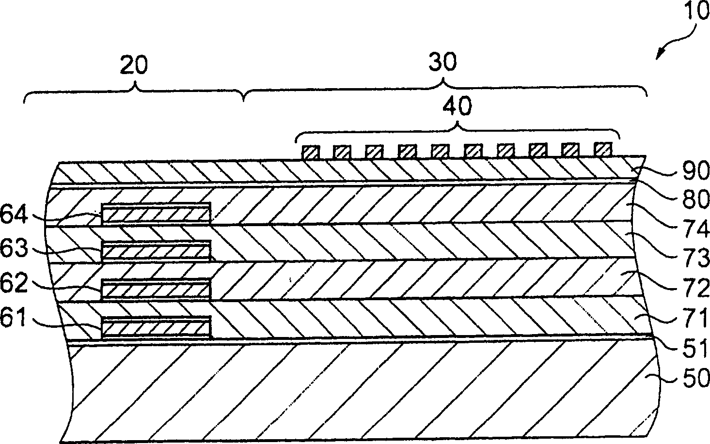
[0035] exist figure 2 shows the surface acoustic wave device 10 of this embodiment figure 1 Use the partial cross-sectional view shown in A-A. exist figure 2 In the surface acoustic wave device 10,...

Embodiment approach 2

[0068] Next, a surface acoustic wave device according to Embodiment 2 of the present invention will be described with reference to the drawings. Embodiment 2 is based on the technical idea of ​​Embodiment 1 described above, and particularly aims at improving the uniformity of the thickness of the insulating layer in the SAW region of the surface acoustic wave element formed on the outer peripheral portion of the wafer.

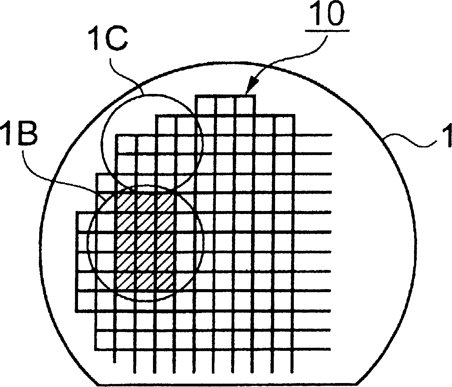
[0069] exist Figure 9 shows the surface acoustic wave device of Embodiment 2, Figure 9 (a) is a partial plan view showing the arrangement of the surface acoustic wave element 10 in the wafer 1, enlarged and schematically shown image 3 1C region shown. exist Figure 9 (b) shows along the Figure 9 (a) The cross-sectional view of the B-B line shown in Figure 9 (c) shows a cross-sectional view along line C-C. exist Figure 9 (a)~ Figure 9 In (c), the metal wiring layer 21 is formed on the outer peripheral portion of the surface acoustic wave element ...

Embodiment approach 3

[0074] Next, Embodiment 3 of the present invention will be described with reference to the drawings. Embodiment 3 is characterized in that Embodiment 1 (refer to figure 2 ) shows that the formation range of the piezoelectric layer 90 is limited to the SAW region, and other structures are the same as those in Embodiment 1, so descriptions are omitted and the same reference numerals are used.

[0075] exist Figure 10 A cross section of the surface acoustic wave element 10 according to Embodiment 3 is shown in . exist Figure 10 In this example, a protective layer 80 is formed within the range of the SAW region 30 on the uppermost insulating layer 74 , and a piezoelectric layer 90 is formed thereon, and an IDT is formed on the piezoelectric layer 90 .

[0076] According to the structure of the third embodiment, the structures and manufacturing methods of the aluminum wirings 61 to 64 and the insulating layers 71 to 74 are the same as those of the first embodiment, and the su...


PUM


Abstract

Surface acoustic wave element and its manufacturing method. An object of the present invention is to provide a surface acoustic wave element having excellent frequency characteristics and pass characteristics, and a method of manufacturing the surface acoustic wave element. As a solution, the surface acoustic wave element (10) is formed with a semiconductor wiring region (20) and a SAW region (30) side by side on the same plane of the semiconductor substrate (silicon layer 50), and a grid pattern is formed on the wafer (1). Arranging the surface acoustic wave element (10), and arranging the semiconductor wiring regions (20) and the SAW regions (30) formed on the adjacent surface acoustic wave elements (10) in an alternate grid pattern, in the semiconductor wiring region (20) Insulating layers (71-74) on the same plane are formed on the top of the SAW region (30), and a piezoelectric layer (90) is formed on the surface of the uppermost insulating layer (74). In the SAW region (30) An IDT (40) is formed on the surface of the piezoelectric layer (90).

Description

technical field [0001] The present invention relates to a surface acoustic wave element formed on a semiconductor substrate and a method for manufacturing the surface acoustic wave element. Background technique [0002] In conventionally known surface acoustic wave devices and their manufacturing methods, an epitaxial layer and a SiO layer are sequentially formed on a semiconductor substrate such as a silicon substrate. 2 layer, on SiO 2 On the upper surface of the layer, a semiconductor wiring region and a SAW (Surface Acoustic Wave, Surface Acoustic Wave) region are arranged in parallel with the plane direction. In the SAW region, SiO 2 thicker SiO 2 A comb-shaped IDT (Interdigital Transducer, interdigital transducer) made of aluminum and a piezoelectric layer (ZnO) are formed on the layer, and in the semiconductor wiring area, SiO 2 layer formed on top of the aluminum wiring layer and silicon nitride (Si 3 N 4 ) composed of an insulating layer (for example, refer to ...

Claims


Application Information

Patent Timeline
Patent Type & Authority Applications(China)
IPC IPC(8): H03H9/25H03H9/64
Inventor 古畑诚后藤健次佐藤久克
Owner SEIKO EPSON CORP
Why Eureka
Try Eureka