Ceramic capacitor and its manufacturing method and electric medium laminated device

A technology of ceramic capacitors and dielectric layers, which is applied in the field of dielectric laminated devices, the manufacture of ceramic capacitors, and low-capacity ceramic capacitors, and can solve the problems of unavoidable stack offsets and other issues

Inactive Publication Date: 2004-05-19
PANASONIC CORP
View PDF2 Cites 0 Cited by
  • Summary
  • Abstract
  • Description
  • Claims
  • Application Information

AI Technical Summary

Problems solved by technology

On the other hand, stack shift cannot be avoided as long as the board stack-up method is used
Therefore, the miniaturization of the

Method used


Image

  • Ceramic capacitor and its manufacturing method and electric medium laminated device
  • Ceramic capacitor and its manufacturing method and electric medium laminated device
  • Ceramic capacitor and its manufacturing method and electric medium laminated device

Examples


Embodiment approach 2

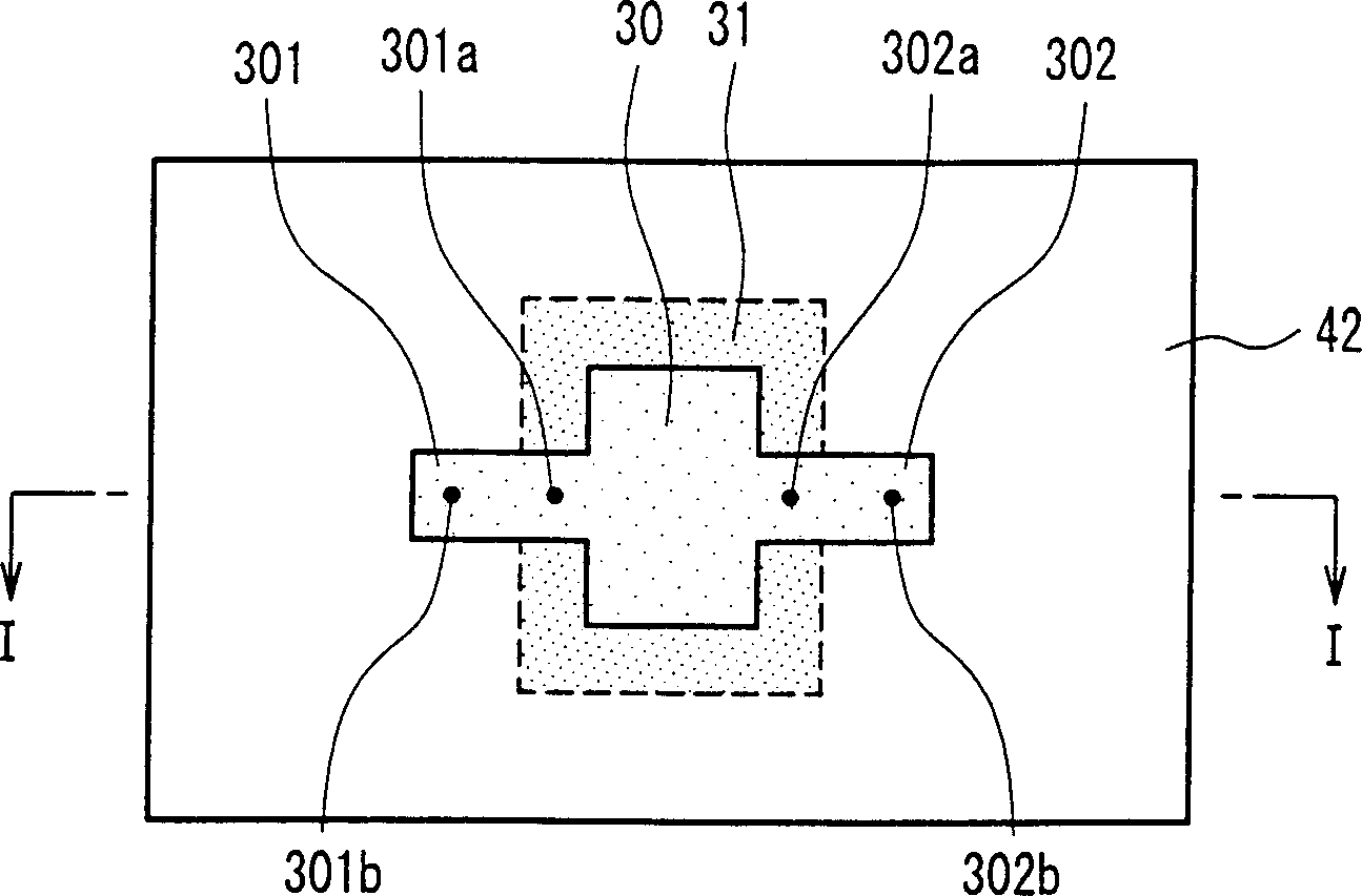
[0095] Figure 5 It is a projected view seen in the thickness direction of the dielectric layer of the ceramic capacitor according to the second embodiment. Figure 6 is along Figure 5 Sectional view of the line II-II.

[0096] Such as Figure 5 and Figure 6 As shown, the ceramic capacitor according to Embodiment 2 has a dielectric layer 42 . In the thickness direction of the dielectric layer 42, the first conductor pattern 36 and the second conductor pattern 37 are arranged to face each other, sandwiching the dielectric layer 42 therebetween. An opening 36 a penetrating in the same direction as the thickness direction of the dielectric layer 42 is provided in the first conductor pattern 36 .

[0097] When projected in the thickness direction of the dielectric layer 42, the second conductor pattern 37 is formed in a stripe pattern, the center portion spans the opening 36a, and both ends 37a, 37b overlap the first conductor pattern 36. The strip-shaped second conductor ...

Embodiment approach 3

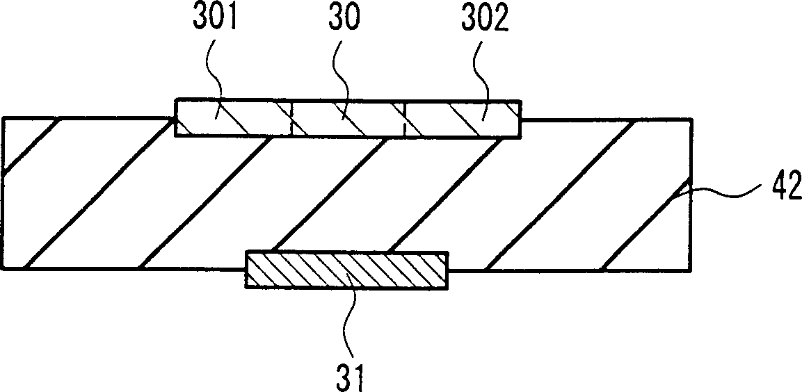
[0107] Figure 9 It is a projected view in the thickness direction of the dielectric layer of the ceramic capacitor according to the third embodiment. Figure 10 is along Figure 9 Sectional view of line III-III.

[0108] Except for the following points, since the ceramic capacitor according to Embodiment 3 is the same as the ceramic capacitor according to Embodiment 2, the same or corresponding parts are denoted by the same symbols, and description thereof will not be repeated. exist Figure 9 ~ Figure 10 Among them, 37 is the body part of the second conductor pattern (abbreviated as "second conductor pattern"), and 37a and 37b are its extension parts. 37c is a swollen portion at the center of the second conductor pattern 37 .

[0109] The difference between the ceramic capacitor according to Embodiment 3 and the ceramic capacitor according to Embodiment 2 is that, as Figure 9 As shown, one end of the second conductor pattern 37 is integrally formed with a third conduct...

Embodiment 1

[0115] This example was performed to confirm the effects of the invention according to Embodiment 1 through experiments.

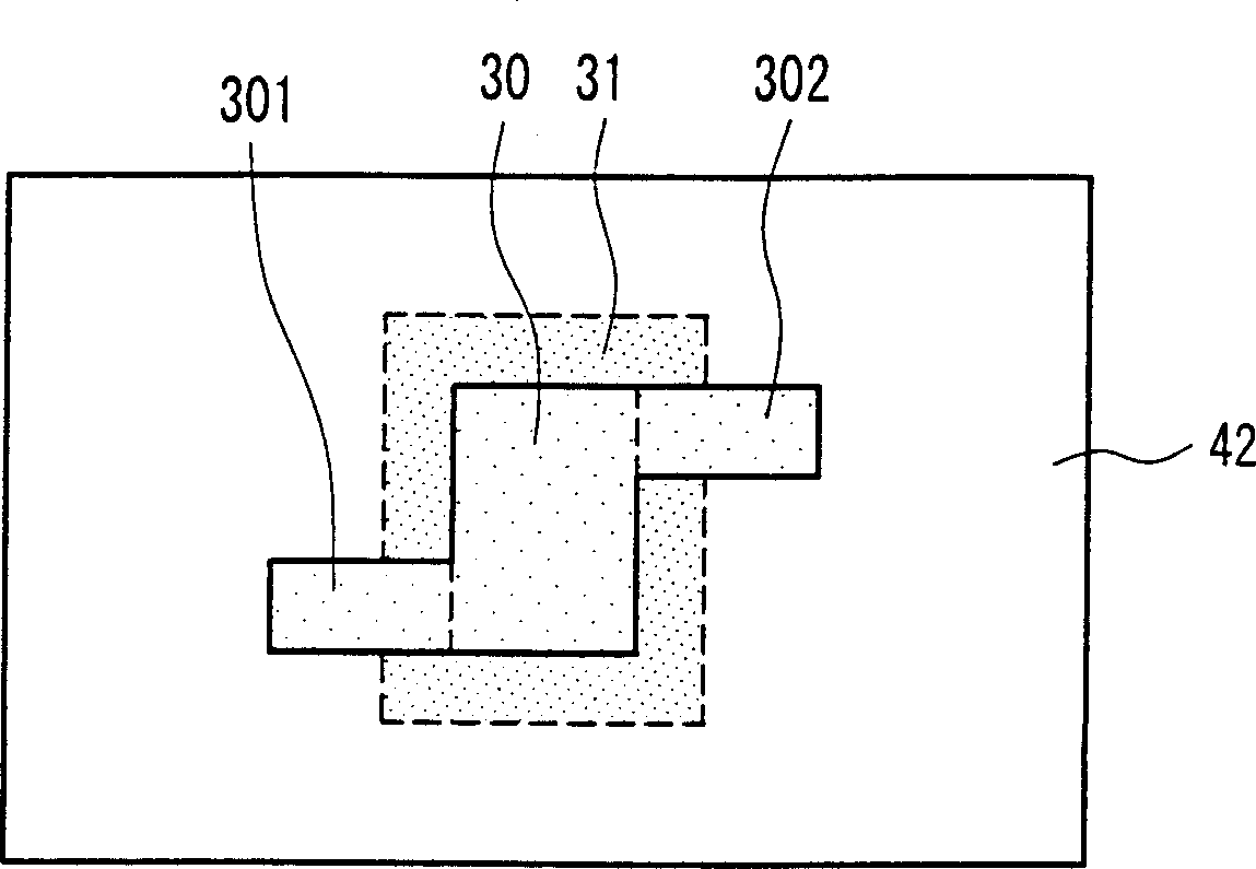
[0116] Figure 11A It is a projected view in the thickness direction of a dielectric layer of the ceramic capacitor which concerns on a comparative example. The ceramic capacitor according to the comparative example has a first conductor pattern 31 and a second conductor pattern 30, and on the second conductor pattern 30, an extension 302 is provided only at one end thereof.

[0117] Figure 11B It is a projection view of the ceramic capacitor according to the first embodiment in the thickness direction of the dielectric layer. The ceramic capacitor according to Embodiment 1 has a first conductor pattern 31 and a second conductor pattern 30 , and at both ends of the second conductor pattern 30 , extensions 301 and 302 extending in opposite directions are provided. These extend outward from the outer peripheral edge of the first conductor pattern 31, res...


PUM


Abstract

A ceramic capacitor includes: a first conductive pattern; a second conductive pattern and a dielectric layer, the first conductive pattern and the second conductive pattern being made of a conductor and provided so as to oppose each other and sandwich the dielectric layer therebetween. The first conductive pattern and the second conductive pattern are different in area from each other, where the second conductive pattern is smaller than the first conductive pattern, and a portion where the first conductive pattern and the second conductive pattern overlap each other forms a capacitance portion. A first extended portion and a second extended portion made of the conductor are formed at both edges of the second conductive pattern so as to extend in mutually opposite directions. With this configuration, the ceramic capacitor with a reduced variation in capacitance value caused by displacement in lamination of green sheets can be provided.

Description

technical field [0001] The present invention relates to general ceramic capacitors, in particular to an improved low-capacity ceramic capacitor with good repeatability and mass production of the same characteristics. The present invention also relates to an improved method of manufacturing low capacitance ceramic capacitors with increased yield. The present invention also relates to an improved dielectric multilayer device using the above-mentioned ceramic capacitor and having stable frequency characteristics. Background technique [0002] Conventionally, ceramic capacitors and dielectric multilayer devices using the ceramic capacitors have been mainly used in communication equipment. Figure 16 This is a block diagram of a communication device such as a mobile phone that incorporates a dielectric multilayer device such as a filter. A mobile phone has a transmitter 100 , a receiver 101 , a baseband unit 11 , a duplexer 2 , a radiator 6 and an antenna 1 . The transmitter 10...

Claims


Application Information

Patent Timeline
IPC IPC(8): H01G4/005H01G4/12H01G4/30
Inventor 竹内孝之山冈正拓川原惠美子
Owner PANASONIC CORP
Why Eureka
Try Eureka