ESD protection device for semiconductor products

A semiconductor and product technology, applied in the field of electrostatic discharge protection devices, can solve problems such as sharp drop in gate breakdown voltage

Inactive Publication Date: 2006-06-14
FAIRCHILD SEMICON CORP
View PDF1 Cites 6 Cited by
  • Summary
  • Abstract
  • Description
  • Claims
  • Application Information

AI Technical Summary

Problems solved by technology

[0009] Another trend limiting the performance of ESD protection circuitry involves the drastic drop in gate breakdown voltage

Method used


Image

  • ESD protection device for semiconductor products
  • ESD protection device for semiconductor products
  • ESD protection device for semiconductor products

Examples


Embodiment Construction

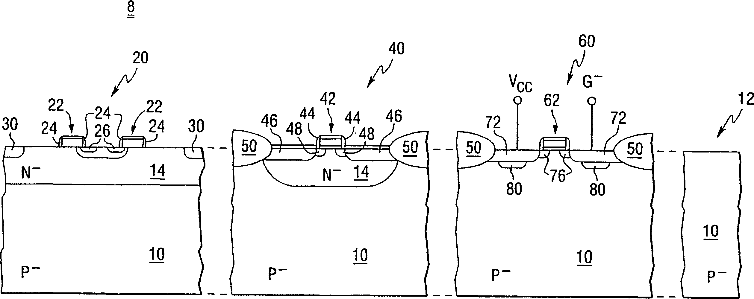
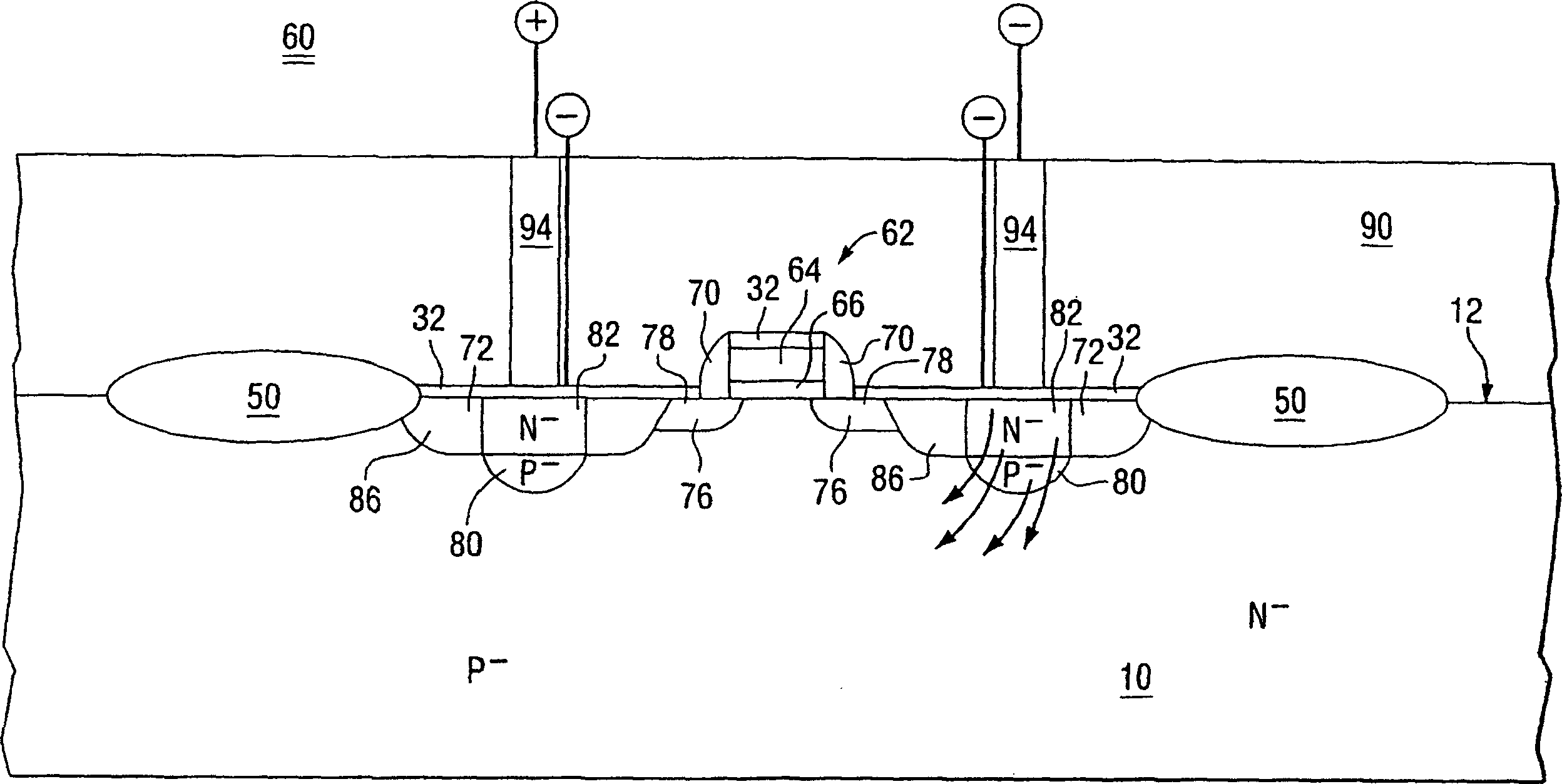
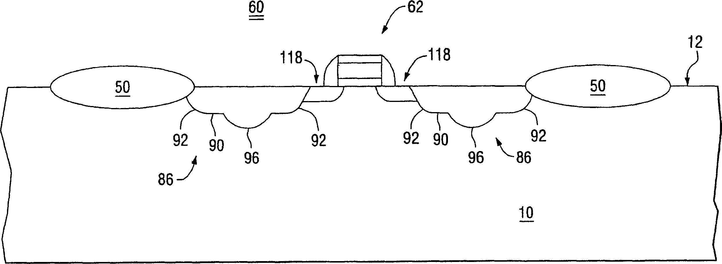
[0019] In the following description, any dimensions given are relative to distances taken along the corresponding figure. In cross-sectional views, the width of a lateral dimension refers to the distance along a horizontal plane parallel to the planar semiconductor surface, and the height or depth refers to the distance taken in a direction perpendicular to the drawing, generally perpendicular to the planar semiconductor surface. For purposes of comparison with known designs, it is assumed in the embodiments of the present invention that all devices illustrated are fabricated with the same lithographic technique. The embodiments disclosed here take the smallest device size, that is, a line width geometry of 0.35 microns, but the present invention is applicable to a wide range of line width geometries, device densities, and various semiconductor products.

[0020] The term substrate is used here to mean a layer on or in which a structure such as a transistor device is formed, a...


PUM


Abstract

The device (60) in Figure 3 has knots (86) each having a transverse portion (90) and a second portion (92) extending from the transverse portion towards the surface (12). The lateral portion (90) is formed generally along a plane parallel to the surface (12) as shown in Figure 3 . The second portion (92) includes the characteristic curved edge of the diffusion front associated with the planarization process. Since the regions (80 and 82) each have a higher net doping concentration of a different conductivity type, each lateral junction portion (90) includes a sub-region (96) deeper into the layer (10). The sub-region (96) is characterized by a lower breakdown voltage compared to the rest of the junction (86), such that the ESD current is initially directed vertically 50 rather than laterally.

Description

technical field [0001] The present invention relates to semiconductor devices, and more particularly to electrostatic discharge (ESD) protection devices for integrated circuit systems. Background technique [0002] Field-effect transistors (FETs) have become the most versatile devices in integrated circuit systems, but they are responsible for a wide range of electronic fields, such as analog signal processing, memory functions, high-speed, low-power logic operations, and power conversion. [0003] Over the past decade, the semiconductor industry has focused more fully on the application of protection circuitry to protect FETs and other circuitry from simple high power voltage spikes such as SEDs. Since FET is a widely used type of device in this type of circuit system in many cases. Therefore, it is most convenient to form the transistor protection device while manufacturing the FET. In this way, additional production steps can be avoided economically. [0004] Although ...

Claims


Application Information

Patent Timeline
Patent Type & Authority Applications(China)
IPC IPC(8): H01L23/62H01LH01L21/338H01L27/02H01L29/76H01L29/78
CPCH01L27/0266H01L29/7833
Inventor 蔡军阿尔文·叙热曼史蒂文·派克
Owner FAIRCHILD SEMICON CORP
Why Eureka
Try Eureka