

Method of testing room temperature press-in creeping performance of metal film
A metal thin film, creep performance technology, applied in the direction of testing the ductility of materials, testing the strength of materials by applying repetitive force/pulsation force, special data processing applications, etc., can solve the difficult application of electronic thin film creep failure testing, mechanical Performance impact, significant surface effect and other issues, to achieve the effect of easy promotion, reduction of economic loss, and reduction of creep failure rate
- Summary
- Abstract
- Description
- Claims
- Application Information
AI Technical Summary
Problems solved by technology
Method used
Image


Examples
Embodiment 1
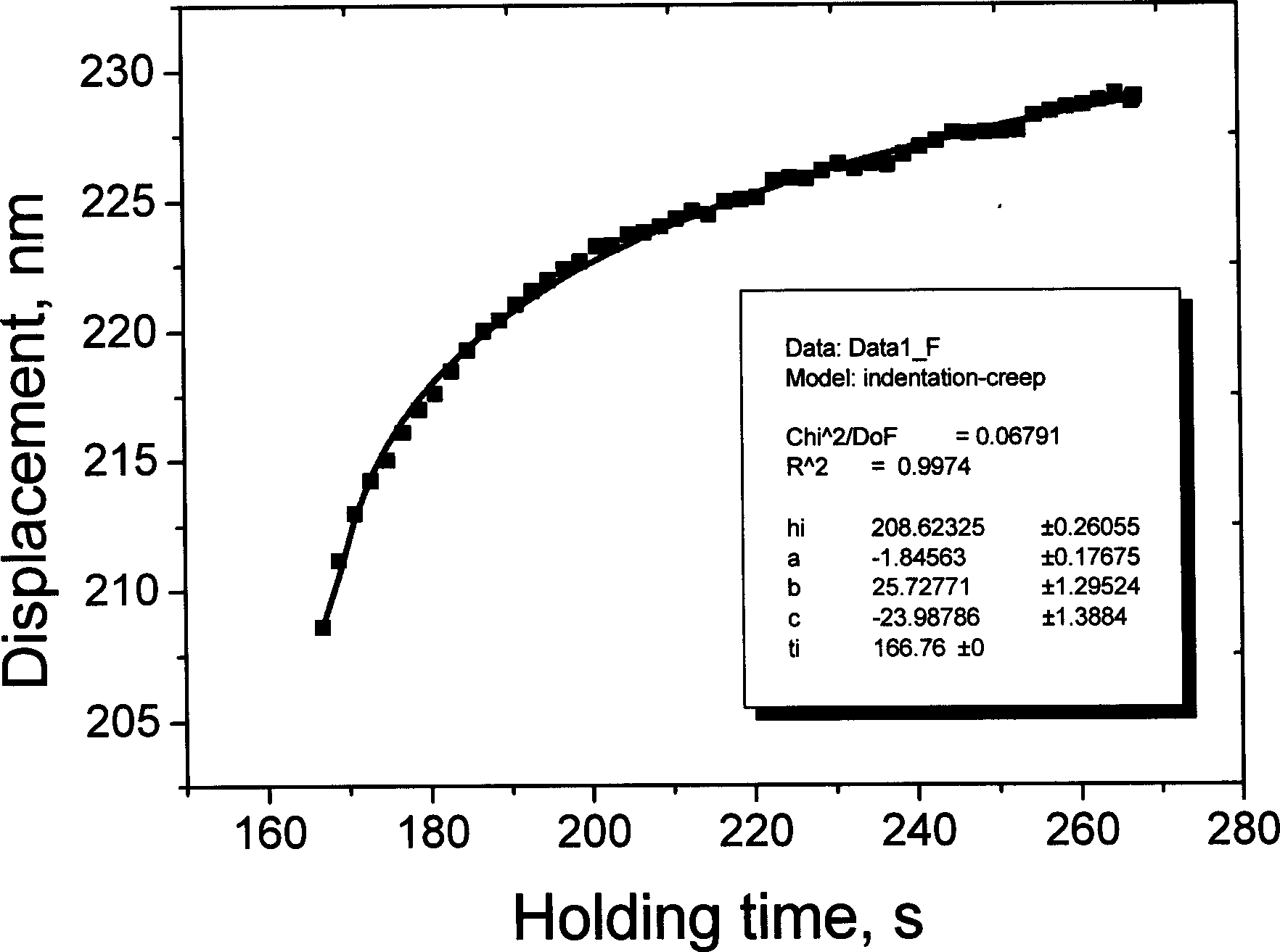
[0029] Using single crystal silicon as the substrate, the metal Cu film was deposited on the silicon wafer at 50°C by using a JGP560V magnetron sputtering apparatus. The substrate was cooled by circulating water, and the thickness of the metal film was controlled to 2 μm. The target purity is greater than 99.99%. The silicon wafer is ultrasonically cleaned before coating. In order to prevent the diffusion between Cu and Si, a layer of 100nm TaN barrier layer is first plated on the silicon wafer, and then Cu is plated. The deposition process parameters of Cu film are: sputtering power 200W; sputtering bias -80V; background pressure 5×10 -5 Pa; working pressure (Ar) 1Pa. Place the sample horizontally on the nanoindenter, using a diamond Berkovish triangular pyramid indenter, with a fixed indentation depth of 200nm and a fixed loading rate of 0.1s -1 , the holding time is 100s, a total of 15 points are measured, and the arithmetic mean value of the stress index is taken. The c...
Embodiment 2
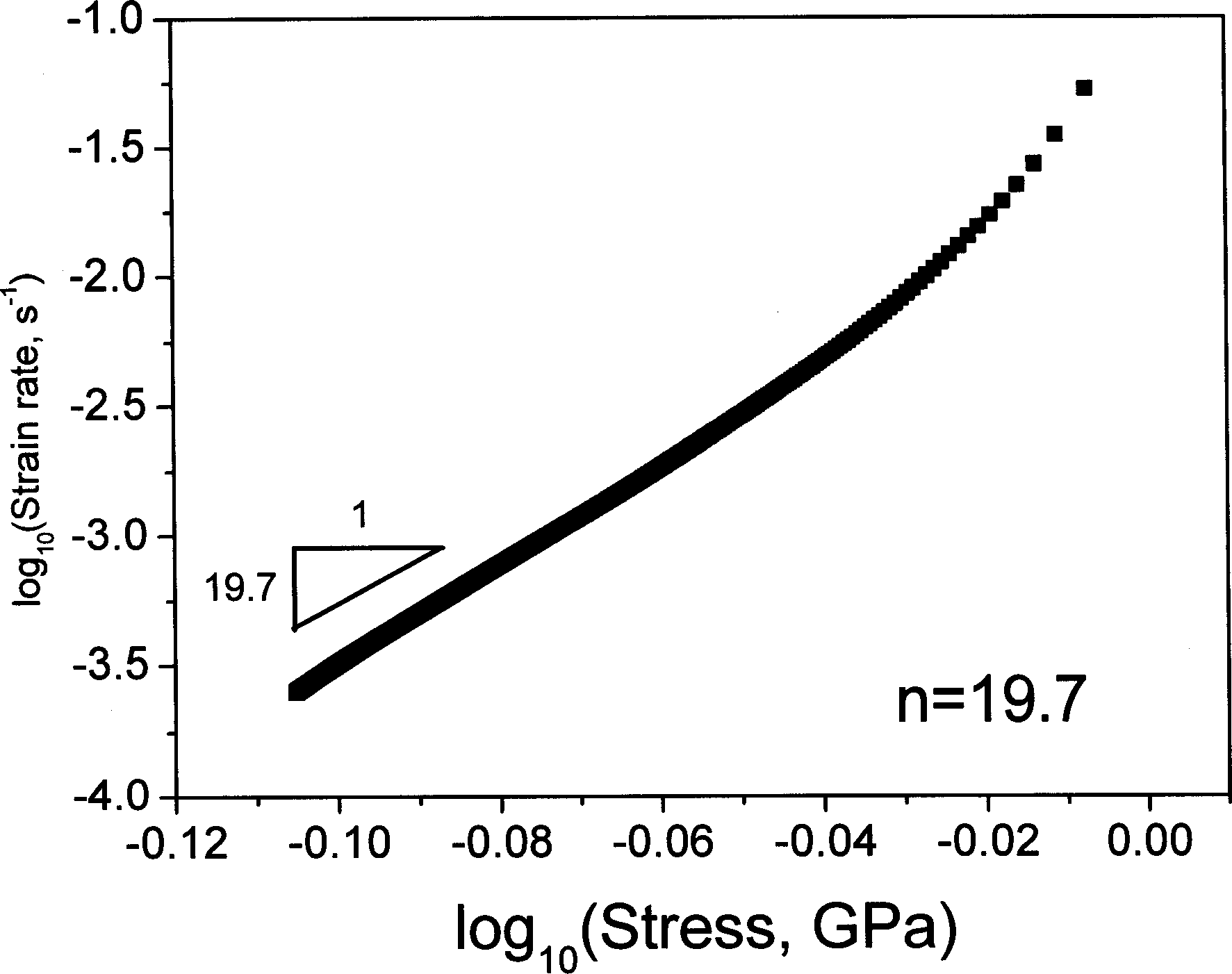
[0031] Take Al 2 o 3 As the substrate, the metal Cu thin film was deposited on the substrate at 40°C by ion beam enhanced assisted deposition technology, and the thickness was controlled to be 3 μm. The deposition process parameters are: bombardment energy 600ev; beam current 60mA; background pressure 1×10 -4 Pa; working pressure (Ar) 0.1Pa. Place the sample horizontally on the nanoindenter, using a diamond Berkovish triangular pyramid indenter, with a fixed indentation depth of 300nm and a fixed loading rate of 0.1s -1 , the holding time is 200s, and a total of 30 points are measured. Measure the displacement-load curve, draw the stress-strain rate curve according to (1) and (2), and its slope is the creep stress index n. In this example, the arithmetic mean value of stress index n=35.1 is taken, which indicates that its creep stability is strong.
Embodiment 3
[0033] With monocrystalline silicon as the substrate, a metal Al film is deposited on a silicon wafer at 50°C by using a JGP560V magnetron sputtering apparatus. The substrate is cooled by circulating water, and the thickness of the film is controlled to 1 μm. The target purity is greater than 99.999%. Before the coating, the silicon wafer was ultrasonically cleaned. In order to prevent the diffusion between Al and Si, a layer of 100nm Ta barrier layer was first coated on the silicon wafer, and then Al was plated. The deposition process parameters of the Al film are: sputtering power 300W; sputtering bias -100V; background pressure 5.7×10 -5 Pa; working pressure (Ar) 0.5Pa. Place the sample horizontally on the nanoindenter, using a diamond Berkovish triangular pyramid indenter, with a fixed indentation depth of 80nm and a fixed loading rate of 0.1s -1 , the holding time is 150s, 30 points are measured in total, according to the measured displacement-load curve, the stress-str...
PUM
| Property | Measurement | Unit |
|---|---|---|
| thickness | aaaaa | aaaaa |
| thickness | aaaaa | aaaaa |
Abstract
Description
Claims
Application Information