Light emitting screen structure and image forming apparatus

A technology of light-emitting screens and light-emitting elements, applied in image/graphic display tubes, discharge tubes, screen tubes, etc., can solve problems such as uneven brightness, device damage, and insufficient solutions.

Inactive Publication Date: 2006-07-12
CANON KK
View PDF3 Cites 1 Cited by
  • Summary
  • Abstract
  • Description
  • Claims
  • Application Information

AI Technical Summary

Problems solved by technology

This discharge current causes damage to the device, so that even if there is no unevenness in brightness as described above, Figure 7 The configuration shown also does not adequately address this shortcoming

Method used


Image

  • Light emitting screen structure and image forming apparatus
  • Light emitting screen structure and image forming apparatus
  • Light emitting screen structure and image forming apparatus

Examples


example 1

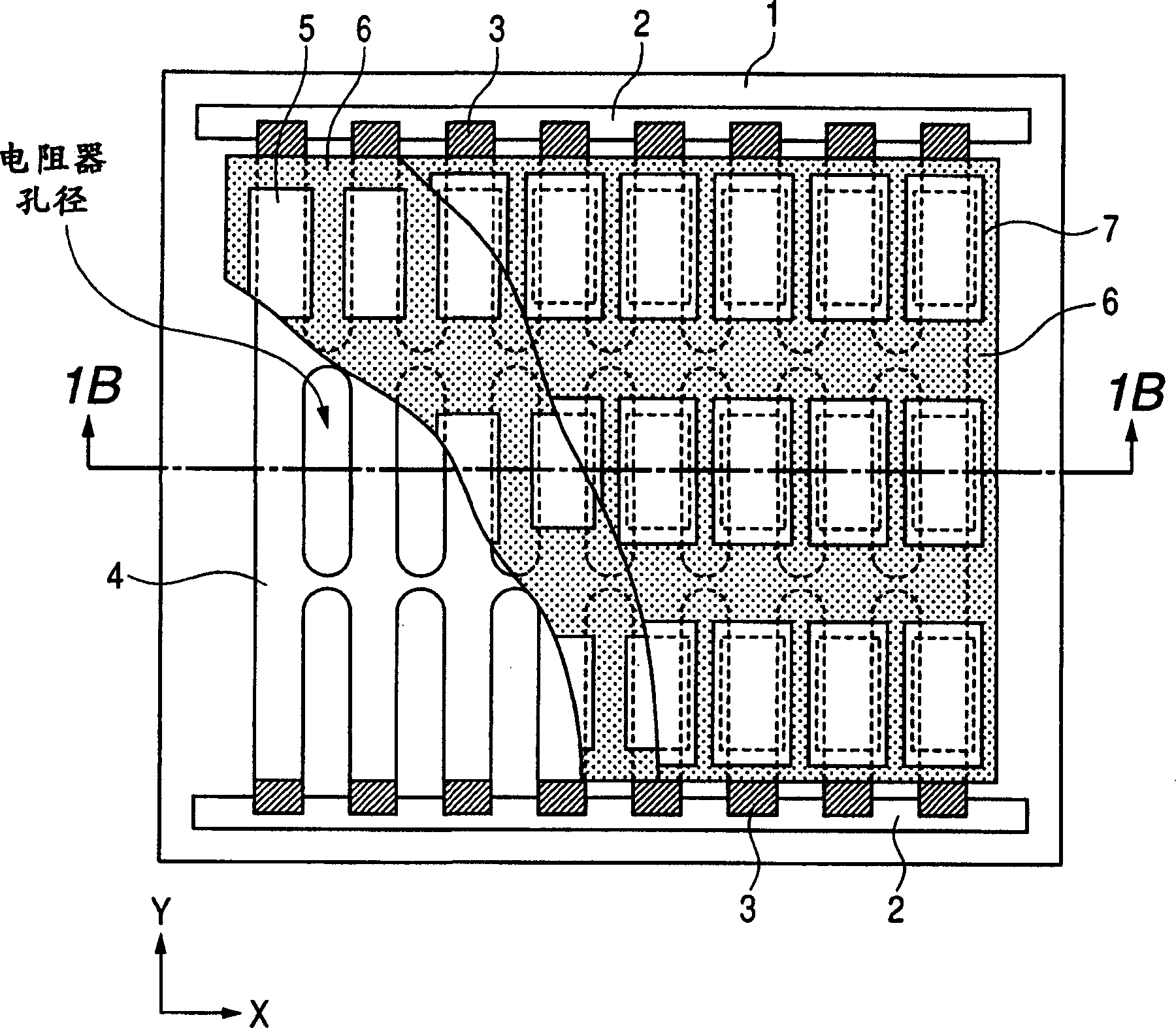
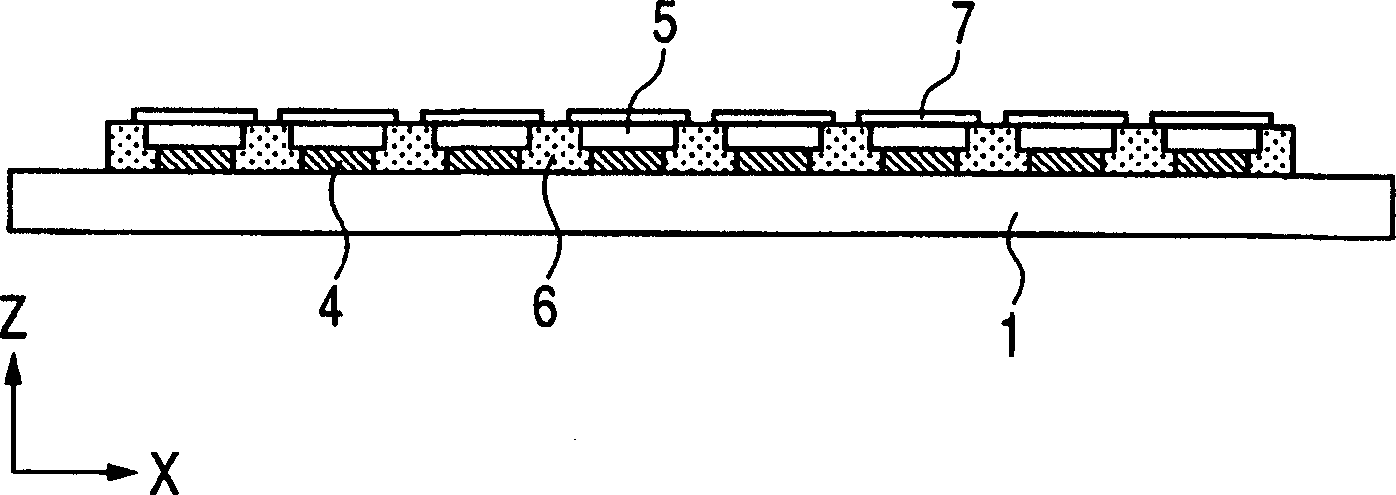
[0062] have as Figure 1A and 1BA light-emitting substrate of the configuration shown was prepared in the following procedure.

[0063] On a glass substrate 1, an ITO film was formed on the entire upper surface, and a grid-shaped pattern was formed by lithographic printing processing, so that a resistor element 4 was obtained. Then, a patterned NiO film was formed as the connection resistor 3 . Then, the common electrode 2 is formed with Ag paste so as to be in contact with all the connection resistors 3 . Then, NP-7803 (manufactured by Noritake Kizai Co., Ltd.) was printed as a black element 6 on the patterned ITO film, followed by coating and baking of red, green and blue phosphors 5 . Finally, an island-shaped metal backplane 7 is formed on the phosphor 5 by vacuum evaporation.

[0064] In this example, a glass substrate PD200 manufactured by Asahi Glass Co., Ltd. with a thickness of 2.8 mm was used. In addition, in the matrix-shaped resistor element 4, the width of th...

example 2

[0072] preparation Figure 3A and 3B The light-emitting substrate in the configuration shown. This example is similar to Example 1, except that three red, green and blue phosphors 5 arranged continuously along the X direction are covered by a single metal back plate 7 together.

[0073] In this example, the width of the Y-direction strip portion extending in the Y-direction of the ITO resistor is 100 μm, and the thickness is 100 nm, and the sheet resistance of the ITO film is adjusted to 30 kΩ / square, so that the adjacent metal in the Y-direction A resistance of about 120 kΩ is obtained between the backplanes 7 . In addition, the width of the ITO film extending in the X direction was 50 μm, so that a resistance (individual resistance) of about 800 kΩ was obtained between adjacent metal back plates in the X direction. In addition, the intersecting portion of the grid pattern of the resistance element 4 has a radius of curvature of 50 μm, matching the narrow strip width in th...

example 3

[0080] preparation Figure 4A and 4B The light-emitting substrate in the configuration shown. This example is similar to Example 1, except that the resistor elements 4 are located below the black elements 6, and two Y-direction strip portions of the resistor elements 4 are provided for each metal backplane along the Y-direction.

[0081] In this example, the width of the ITO resistor and the strip portion in the Y direction is 50 μm, and the sheet resistance of the ITO film is adjusted to 30 kΩ / square, thereby obtaining a resistance of about 120 kΩ between adjacent metal backplanes 7 in the Y direction. resistance. In addition, the width of the X-direction stripe portion of the ITO film was 30 μm, thereby obtaining a resistance (individual resistance) of about 800 kΩ between adjacent metal back plates in the X direction. In addition, the intersecting portion of the grid pattern of the resistance element 4 has a radius of curvature of 50 μm, matching the narrow strip width i...


PUM


Abstract

In a flat type image forming apparatus formed by electron emitting devices, the invention is to provide a light emitting substrate, capable of relaxing influence of an abnormal discharge on the electron emitting devices. On a glass substrate 1 , a resistor member 4 extending in X- and Y-direction, and a black member 6 extending in X- and Y-directions are formed. Phosphors 5 are positioned in apertures of the black member 6 , and are covered by metal backs 7 divided in X- and Y-directions. The metal backs 7 and the resistor member 4 are electrically connected through the black member 6 , and the resistance between the metal backs 7 is defined by the resistor member 4 in the Y-direction in which the adjacent metal backs 7 have a wider gap than in the X-direction.

Description

technical field [0001] The present invention relates to a light-emitting screen structure (light-emitting substrate) for constructing an image-forming device such as an image display device together with electron-emitting devices, and to an image-forming device using such a light-emitting substrate. Background technique [0002] Electron emission devices using electron emission devices have been applied to, for example, imaging devices. For example, there is known a flat type electron beam display panel, which is constituted as follows: an electron source substrate having a plurality of cold cathode electron-emitting devices, a metal back plate or a transparent An anode substrate of the electrode, and a phosphor disposed opposite each other with a gap between the substrates. Compared with the currently popular cathode ray tube (CRT), the flat type electron beam display panel is lighter in weight and larger in size. In addition, it can provide higher brightness and higher i...

Claims


Application Information

Patent Timeline
Patent Type & Authority Applications(China)
IPC IPC(8): H01J29/10H01J29/08H01J31/12
Inventor 铃木纪博山崎康二
Owner CANON KK
Why Eureka
Try Eureka