Output buffer circuit for drive voltage in liquid crystal display drive control chip

An output buffer and drive control technology, applied in static indicators, instruments, etc., can solve the problems of complex output buffer circuit structure, poor stability, large static bias current, etc., to save area, good stability, reduce static The effect of power consumption

Inactive Publication Date: 2006-07-19
NORTHWESTERN POLYTECHNICAL UNIV
View PDF0 Cites 11 Cited by
  • Summary
  • Abstract
  • Description
  • Claims
  • Application Information

AI Technical Summary

Problems solved by technology

[0004] In order to overcome the disadvantages of complex structure, poor stability and large static bias current in the prior art output buffer circuit, the present invention provides an output buffer circuit for driving voltage in a liquid crystal display drive control chip

Method used


Image

  • Output buffer circuit for drive voltage in liquid crystal display drive control chip
  • Output buffer circuit for drive voltage in liquid crystal display drive control chip
  • Output buffer circuit for drive voltage in liquid crystal display drive control chip

Examples


Embodiment Construction

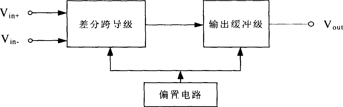
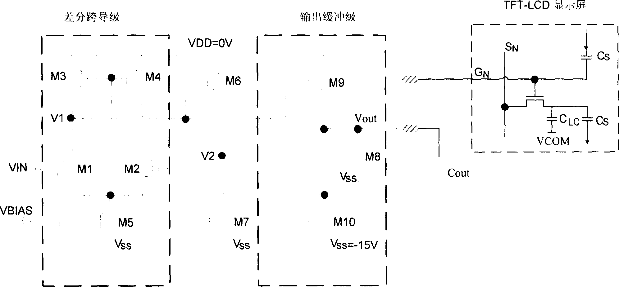
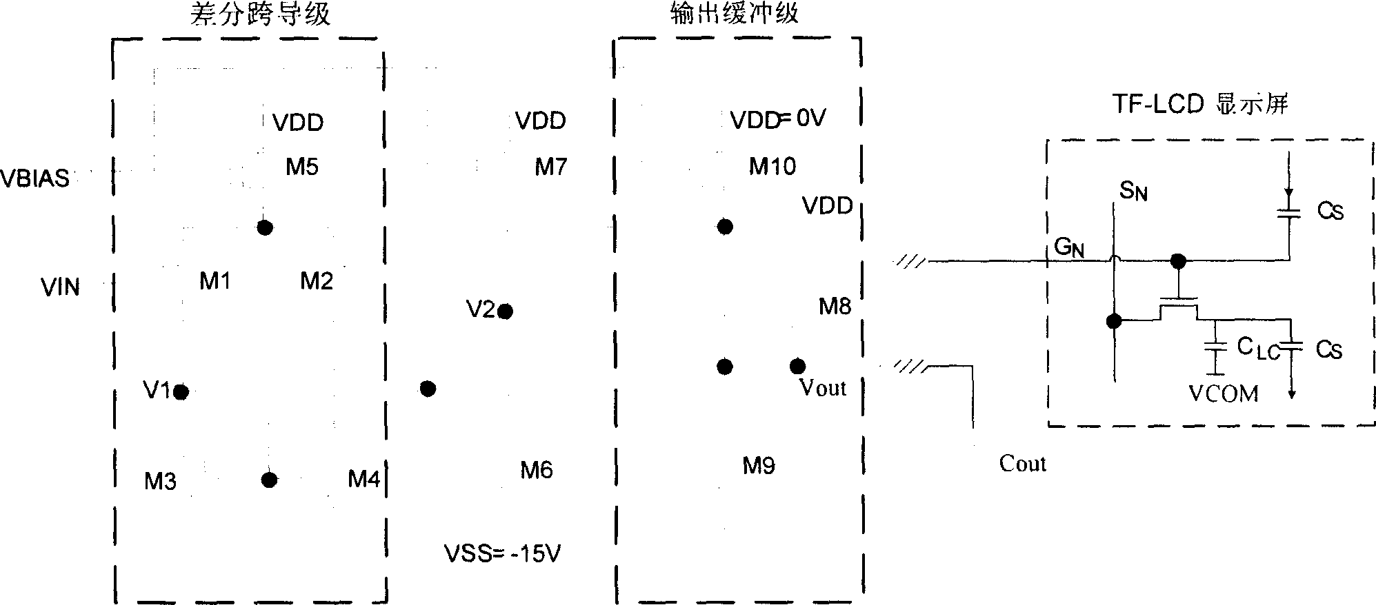
[0017] refer to Figure 1~3 The output buffer circuit of the driving voltage provided by the present invention includes a differential transconductance stage, an output buffer stage two-stage amplifier, and an external bias circuit.

[0018] The output voltage V1 of the differential transconductance stage is directly added to the input terminal of the common source amplifier circuit, and the output terminal of the common source amplifier circuit is connected with the output terminal of the source follower as the output terminal of the output buffer circuit. The output voltage V1 of the differential transconductance stage is added to the floating bias circuit of the source follower at the same time, and the floating bias voltage V2 generated is added to the input terminal of the source follower. The bias circuit provides a fixed DC bias voltage VBIAS to the differential transconductance stage and the output buffer stage.

[0019] The structures and working principles of the ou...


PUM


Abstract

The invention discloses an output buffer circuit which uses liquid crystal display to drive the driving voltage of the control chip. The first level amplifier is a difference mutual admittance circuit which is formed by MOS pipes (M1-M5); the second level amplifier is a common source stage amplifier circuit which is formed by MOS pipes (M9-M10); it adds source electrode follower of MOS pipe (M8) on the output end. It adopts complementary push-pull output circuit, one pipe works at any time, when one pipe stops, 1) when the output voltage stabilizes, MOS pipe (M8) stops, the static deflexed current doesn't follow to the MOS pipe (M8) and the static deflexed current of MOS pipe (M9) is 0.2úÑ of the current technology static deflexed current which can reduce the static power of the circuit; 2) When the MOS pipe (M8) stops, the output buffer circuit is formed by two level amplifiers.

Description

technical field [0001] The invention relates to an output voltage buffer circuit, in particular to an output buffer circuit for driving voltage in a liquid crystal display driving control chip. Background technique [0002] refer to Figure 5-7 , the voltage VCOM is the driving voltage of the common electrode terminal of the TFT-LCD display, and the voltage VGOFF is the Gate turn-off voltage of the non-scanning line. As the VCOM voltage periodically varies between VCOMH and VCOML, the corresponding VGOFF voltage periodically varies between VGOFFH and VGOFFL. Each pixel unit of the TFT-LCD display consists of a thin film transistor TFT, a liquid crystal equivalent capacitance C LC and the storage capacitor Cs, and there is a parasitic capacitance Cgd between the gate and the drain of the thin film transistor TFT. When the Gate of row N+1 changes from off state to on state, the Gate voltage of this row jumps from VGOFF to VGH. Since the Gate of the Nth row is in the off sta...

Claims


Application Information

Patent Timeline
Patent Type & Authority Applications(China)
IPC IPC(8): G02F1/133G09G3/36
Inventor 魏廷存高德远樊晓桠张盛兵罗旻王党辉
Owner NORTHWESTERN POLYTECHNICAL UNIV
Why Eureka
Try Eureka