Atomic beam generation method and apparatus for atomic chipset

A technology of atomic chips and generating devices, applied in phonon exciters, masers, circuits, etc., can solve the problems of low atomic density, low longitudinal velocity, and low transverse velocity, and achieve increased atomic density and velocity distribution Uniform, low transverse velocity effect

Inactive Publication Date: 2006-07-19
TSINGHUA UNIV
View PDF0 Cites 23 Cited by
  • Summary
  • Abstract
  • Description
  • Claims
  • Application Information

AI Technical Summary

Problems solved by technology

Although the atomic source of the Bose-Einstein condensate prepared by this method has the characteristics of good singleness and uniform velocity distribution, the preparation of the Bose-Einstein condensate requires multi-level magneto-optical traps, a large system and a complex structure. The vacuum degree is high, and the adiabatic transportation and chip loading of the atomic beam cannot be well realized. The ultracold atoms have divergence and splash loss when they are transported between the magneto-optical traps, which reduces the system efficiency.
[0004] Due to the low density of atoms that can be controlled by the chip magnetic trap produced by the existing technology, and the trapping ability of the chip magnetic trap is limited to a certain extent, it is hoped that the optimal weak field search state, low longitudinal velocity and uniform distribution can be obtained on the chip surface. Beams of atoms with very low transverse velocity and high density

Method used


Image

  • Atomic beam generation method and apparatus for atomic chipset
  • Atomic beam generation method and apparatus for atomic chipset
  • Atomic beam generation method and apparatus for atomic chipset

Examples


Embodiment Construction

[0088] The present invention will be described in further detail below in conjunction with the accompanying drawings and specific embodiments.

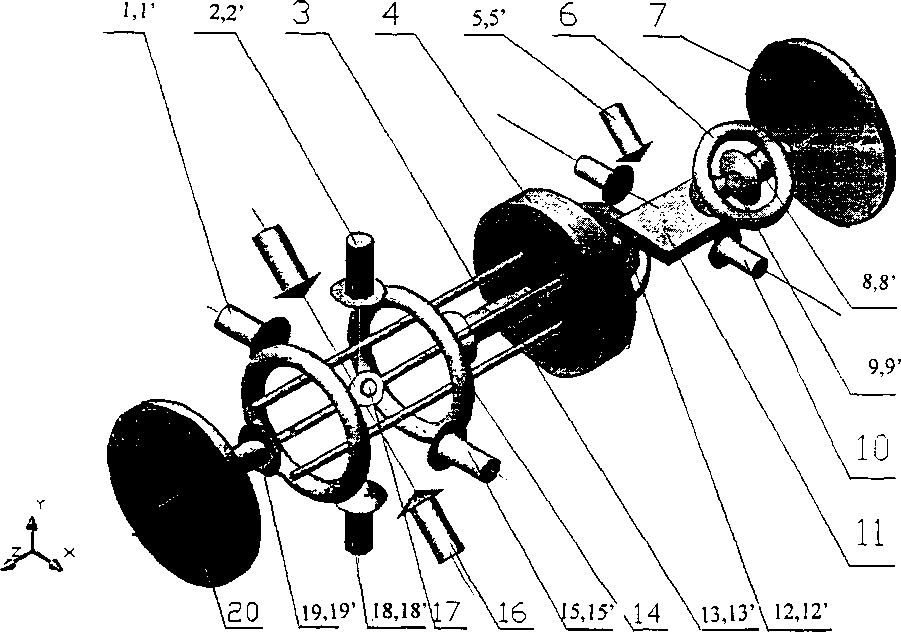
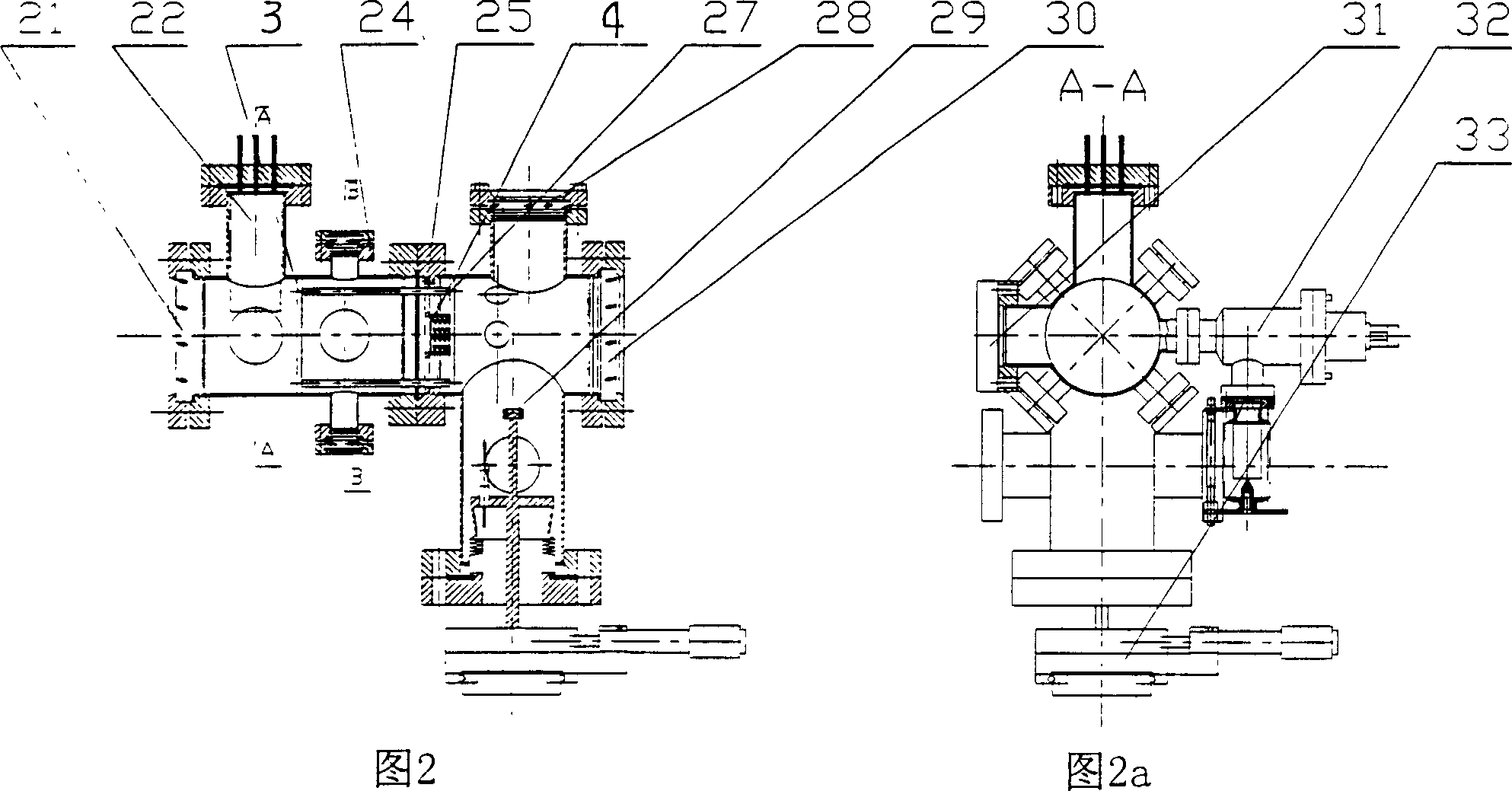
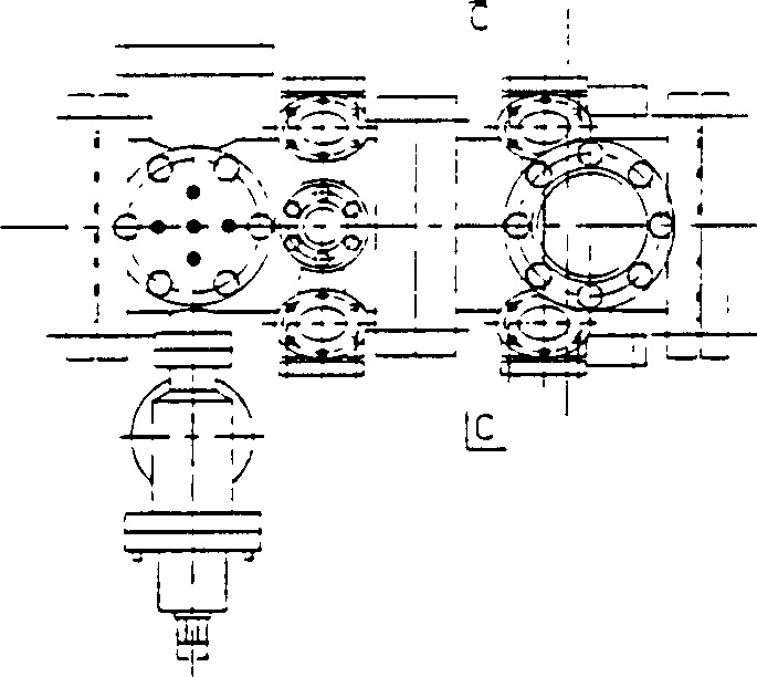
[0089] The atomic beam generating device for an atomic chip provided by the present invention includes an atomic source, a vacuum chamber, a two-dimensional fine-tuning table, a magnet (permanent magnet or magnetic field coil) and an internal and external optical system.

[0090] Such as figure 1 As shown, the three-dimensional magneto-optical trap formed by cooling lasers 1, 2, 13, 15, 18, 19 and the second pair of anti-Hertz coils 14 captures and cools the atom source steam beam 17 ejected from the hot atom source nozzle, Wherein the cooling laser 15 is that the cooling laser 1 passes through a 1 / 4 wave plate positioned outside the vacuum chamber and a mirror ( figure 1 Not shown in ) the reflected cooling laser that obtains, cooling laser 18 is that cooling laser 2 passes through a 1 / 4 wave plate and a mirror ( figure 1 not shown...


PUM


Abstract

The invention relates to a method for generating the atom bean used in atom chip and relative device, wherein, the device comprises a vacuum room, an atom source, a two-dimensional micro adjusting platform, a magnetic iron and inner and outer light paths. The inner and outer light paths comprise a main laser and a re-pump laser; the vacuum room is mounted with a 1/4 wave plate reflector group with a hole in center and a direct-guide group; the magnetic light well uses the optical pump laser and the re-pump laser to prepare the atom into optimized weak field scanning state. The invention has small volume and simple structure, while it can supply the optimized weak field scanning state to the atom chip with the atom beam whose longitudinal speed is lower and uniform, transverse speed is nearly zero and density is high. The invention can be used in the guide, wave-division, interference and the Bose-Einstein Coagulation (BEC).

Description

technical field [0001] The invention provides an atomic beam preparation, transportation and loading device for an atomic chip, especially a device that provides and loads an optimal weak field search state for an atomic chip, has low longitudinal velocity and uniform distribution, almost zero transverse velocity, and high density Generating method and device of atomic beam. Background technique [0002] At present, there are mainly two methods of generating atomic beams used in atomic chips: hot atomic beams and ultracold atomic beams (ie, Bose-Einstein condensates). The hot atomic beam generally heats the atomic source directly to form an atomic steam beam ejected from the nozzle, decelerates it with a laser beam opposite to the velocity direction of the atomic steam beam, and then loads it through a mirror magneto-optical trap (Mirror MOT). To the chip surface, as described in Document 1: J. Denschlag, D. Cassettari, A. Chenetl, S. Schneider, J. Schmiedmayer, Appl. Phys....

Claims


Application Information

Patent Timeline
Patent Type & Authority Applications(China)
IPC IPC(8): H05H3/02
Inventor 叶雄英朱常兴周兆英朱荣冯焱颖唐兴伦杨兴
Owner TSINGHUA UNIV
Why Eureka
Try Eureka