Inner-mould ornamental plastic member capable of being completed by ordinary injection die and its production method
A technology of injection mold and in-mold decoration, which is applied in the fields of technology for producing decorative surface effects, decorative art, chemical instruments and methods, etc. It can solve problems such as poor rigidity, ink layer damage, complex positioning and clamping, etc., to achieve The effect of low design and manufacturing cost, easy stamping and forming, and fast production speed
- Summary
- Abstract
- Description
- Claims
- Application Information
AI Technical Summary
Problems solved by technology
Method used
Image
Examples
Embodiment 1
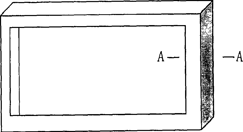
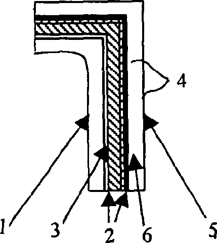
[0036] figure 1 , figure 2 A schematic diagram of the structure of the TV casing in Embodiment 1 is given. see figure 1 , figure 2 The TV casing consists of a plastic base 1, a cold-rolled steel metal layer 3 with a thickness of 0.8 mm that is compounded with the plastic base through an adhesive layer 2, and a decorative flexible layer 4 that is compounded with the metal layer through another adhesive layer 2 composition. The decorative flexible layer 4 is made up of a polycarbonate transparent plastic film 5 with a thickness of 0.4mm and a decorative layer 6 with patterns and characters printed on the transparent plastic film.
[0037] The steps of the manufacturing method of the TV casing of the present embodiment are as follows:
[0038] 1. Print pattern and text decoration layer on one side of polycarbonate transparent plastic film (flexible decorative materials with patterns or decorative effects can also be used, such as printed film, cloth, leather, etc. The foll...
Embodiment 2
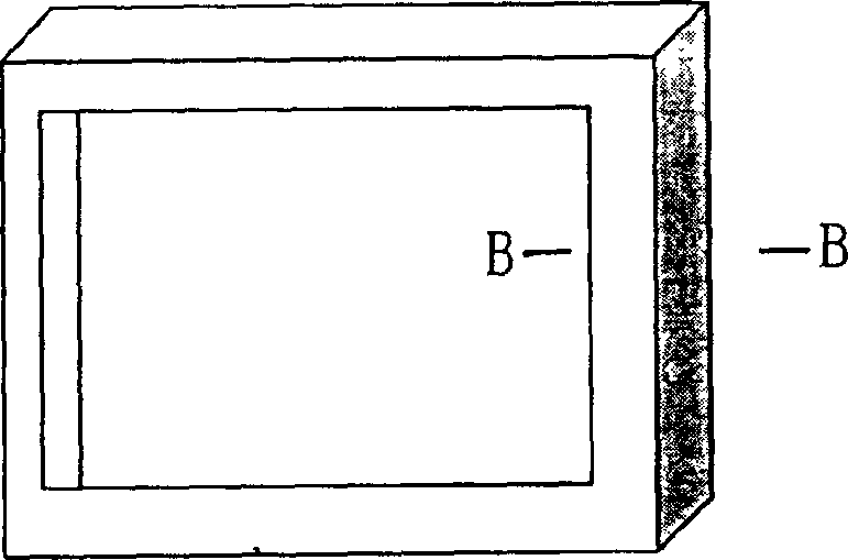
[0044] image 3 , Figure 4 A schematic structural diagram of a computer display case in Embodiment 2 is given. The sectional structure of the display screen casing is basically the same as the sectional structure of the TV casing in Embodiment 1, the difference is that there is no adhesive layer between the plastic substrate and the metal layer, the thickness of the metal layer is 0.6mm, and the plastic film layer The thickness is 0.3mm. The manufacturing method of the display screen casing is basically the same as that of embodiment 1, except that in step 2, only the adhesive layer is coated on one side of the metal sheet.
Embodiment 3
[0046] Figure 5 , Figure 6A schematic diagram of the frame structure of the communication device in Embodiment 3 is given. The cross-sectional structure of the face frame of the communication device is basically the same as that of Embodiment 2, except that there is no adhesive layer between the flexible decoration layer and the metal layer, the thickness of the metal layer is 0.4 mm, and the thickness of the plastic film layer is 0.18 mm. The manufacturing method of the surface frame of the communication equipment in the third embodiment is basically the same as that in the second embodiment, except that the process of coating the adhesive layer on the metal sheet is omitted.
PUM
| Property | Measurement | Unit |
|---|---|---|
| thickness | aaaaa | aaaaa |
| thickness | aaaaa | aaaaa |
| thickness | aaaaa | aaaaa |
Abstract
Description
Claims
Application Information
 - R&D
- Intellectual Property
- Life Sciences
- Materials
- Tech Scout
- Unparalleled Data Quality
- Higher Quality Content
- 60% Fewer Hallucinations
Browse by: Latest US Patents, China's latest patents, Technical Efficacy Thesaurus, Application Domain, Technology Topic, Popular Technical Reports.
© 2025 PatSnap. All rights reserved.Legal|Privacy policy|Modern Slavery Act Transparency Statement|Sitemap|About US| Contact US: help@patsnap.com


